Generic selectors
Exact matches only
Search in title
Search in content
Post Type Selectors

VD0801 Iron Disilicide Evaporation Materials, FeSi2

Catalog No.VD0801
MaterialIron Silicon (FeSi2)
Purity99.9% ~ 99.99%
ShapePowder/ Granule/ Custom-made

TFM stands out as a premier producer and supplier of high-purity iron disilicide evaporation materials, alongside a diverse range of other evaporation materials. Our offerings include both powder and granule forms, with the added flexibility to provide customized options tailored to your specific needs. Whether you require standard or bespoke solutions, TFM delivers exceptional quality and precision in every product.

Iron Disilicide Evaporation Materials Overview

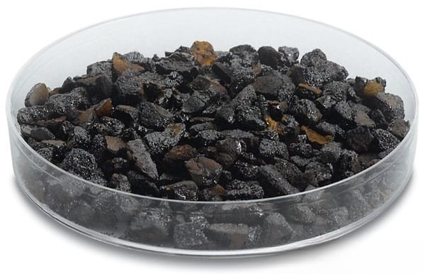
TFM offers high-quality iron disilicide evaporation materials, composed of the silicide ceramic with the formula FeSi2. These high-purity materials, with purity levels reaching up to 99.9995%, are essential for achieving superior quality in deposited films. Our rigorous quality assurance processes ensure the reliability and excellence of our products.

Iron Disilicide Evaporation Materials Specification

Material TypeFerrosilicon
SymbolFeSi2
Appearance/ColorGray tetragonal crystals
Melting Point1,220 °C (2,230 °F; 1,490 K)
Density4.74 g/cm3
Purity99.9% ~ 99.99%
ShapePowder/ Granule/ Custom-made

Iron Disilicide Evaporation Materials Application

Iron disilicide evaporation materials are pivotal in various deposition processes such as semiconductor deposition, chemical vapor deposition (CVD), and physical vapor deposition (PVD). They are widely used in optics for applications including wear protection, decorative coatings, and display technologies.

Packaging and Handling

To ensure optimal quality and ease of use, our iron disilicide evaporation materials are meticulously tagged and labeled. We take extensive precautions to prevent damage during storage and transportation.

Contact Us

TFM is a leading provider of high-purity iron disilicide evaporation materials. We offer various forms including tablets, granules, rods, and wires, with customization options available upon request. Additionally, we supply evaporation sources, boats, filaments, crucibles, heaters, and e-beam crucible liners. For inquiries regarding current prices or materials not listed, please reach out to us directly.

Reviews

There are no reviews yet.

Be the first to review “VD0801 Iron Disilicide Evaporation Materials, FeSi2”

Your email address will not be published. Required fields are marked *

FAQ

  • They are high‐purity substances (e.g. metals, alloys, or compounds) used in thermal or electron‐beam evaporation processes to form thin films on substrates.

  • Typically, they’re processed into a form (often ingots, pellets, or wires) that can be efficiently vaporized. Preparation emphasizes high purity and controlled composition to ensure film quality.

  • Thermal evaporation and electron-beam (e-beam) evaporation are the two main techniques, where material is heated (or bombarded with electrons) until it vaporizes and then condenses on the substrate.

  • Thermal evaporation heats the material directly (often using a resistive heater), while e-beam evaporation uses a focused electron beam to locally heat and vaporize the source material—each method offering different control and energy efficiency.

  • Key parameters include source temperature, vacuum level, deposition rate, substrate temperature, and the distance between the source and the substrate. These factors influence film uniformity, adhesion, and microstructure.

  • Evaporation generally produces high-purity films with excellent control over thickness, and it is especially suitable for materials with relatively low melting points or high vapor pressures.

  • Challenges include issues with step coverage (due to line-of-sight deposition), shadowing effects on complex topographies, and possible re-evaporation of material from the substrate if temperature isn’t properly controlled.

  • Common evaporation materials include noble metals (e.g., gold, silver), semiconductors (e.g., silicon, germanium), metal oxides, and organic compounds—each chosen for its specific optical, electrical, or mechanical properties.

  • Selection depends on desired film properties (conductivity, optical transparency, adhesion), compatibility with the evaporation process, and the final device application (semiconductor, optical coating, etc.).

  • Optimizing substrate temperature, deposition rate, and chamber vacuum are critical for ensuring that the film adheres well and forms the intended microstructure without defects.

  • Troubleshooting may involve checking the source material’s purity, ensuring stable source temperature, verifying the vacuum level, adjusting the substrate’s position or temperature, and monitoring deposition rate fluctuations.

While evaporation tends to yield very high purity films with excellent thickness control, it is limited by its line-of-sight nature. In contrast, sputtering can deposit films more uniformly on complex surfaces and is more versatile for a broader range of materials.


Shopping Cart
Scroll to Top