
 MSDS File
Introduction
Iron Nickel Evaporation Materials (Fe/Ni) are alloy-based sources used in vacuum deposition processes to fabricate magnetic, conductive, and functional metallic thin films. By combining iron’s strong magnetic properties with nickel’s corrosion resistance and structural stability, Fe/Ni alloys are widely utilized in electronics, magnetic devices, shielding applications, and research-scale thin film development.
Fe/Ni evaporation materials provide controlled alloy composition transfer during thermal or electron beam evaporation, enabling precise tuning of magnetic permeability, resistivity, and mechanical characteristics in deposited films.
Detailed Description
Iron Nickel alloys are typically produced through vacuum induction melting or controlled atmosphere melting to ensure homogeneous microstructure and consistent elemental distribution. Common compositions include:
Fe 80% / Ni 20%
Fe 50% / Ni 50%
Fe 36% / Ni 64% (Invar-type composition)
Custom weight or atomic ratios upon request
The selected alloy ratio directly influences magnetic saturation, coercivity, thermal expansion, and electrical conductivity.
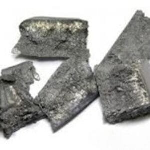
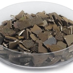
Available forms include:
Pellets
Granules
Alloy pieces
Custom-machined slugs
With melting temperatures generally ranging from approximately 1430–1530°C (depending on composition), Fe/Ni alloys are compatible with electron beam evaporation and high-temperature thermal evaporation systems. Uniform alloy microstructure ensures stable evaporation rates and reduces compositional segregation.
Key material characteristics include:
Tunable magnetic properties
Moderate electrical conductivity
Good adhesion to metallic and semiconductor substrates
Compatibility with multilayer thin film stacks
Fe/Ni alloys are often used where controlled magnetic response or thermal expansion behavior is required.
Applications
Iron Nickel Evaporation Materials are commonly applied in:
Magnetic thin films and soft magnetic layers
MEMS and sensor devices
Electromagnetic shielding coatings
Low thermal expansion (Invar-type) thin films
Microelectronic barrier layers
Research in magnetic and functional alloy films
Precision instrument coatings
In precision instrumentation, Fe/Ni films may be used where dimensional stability under temperature variation is critical.
Technical Parameters
| Parameter | Typical Value / Range | Importance |
|---|---|---|
| Composition | Fe/Ni (custom ratios) | Controls magnetic & thermal properties |
| Purity | 99.9% – 99.99% | Improves film uniformity |
| Form | Pellets / Granules / Pieces | Compatible with evaporation sources |
| Melting Range | ~1430–1530°C | Suitable for e-beam evaporation |
| Density | ~8.1–8.7 g/cm³ (composition dependent) | Relevant for deposition rate control |
| Deposition Method | Thermal / E-beam Evaporation | Enables uniform alloy film growth |
Custom alloy compositions and sizes can be supplied to match specific deposition systems and application requirements.
Comparison with Related Alloy Materials
| Material | Key Advantage | Typical Application |
|---|---|---|
| Iron Nickel (Fe/Ni) | Tunable magnetic properties | Magnetic thin films |
| Pure Iron | Strong magnetic saturation | Magnetic components |
| Pure Nickel | Corrosion resistance | Protective coatings |
| Permalloy (Ni-Fe specific ratio) | High magnetic permeability | Magnetic shielding |
Compared to pure iron or nickel, Fe/Ni alloys offer adjustable magnetic characteristics and improved mechanical balance.
FAQ
| Question | Answer |
|---|---|
| Can the Fe/Ni ratio be customized? | Yes, composition can be tailored to meet magnetic or thermal requirements. |
| Is electron beam evaporation recommended? | Yes, due to high melting temperatures, e-beam evaporation is commonly preferred. |
| Will the alloy composition remain stable during evaporation? | With proper process control, consistent composition transfer can be achieved. |
| Is it suitable for magnetic film applications? | Yes, Fe/Ni alloys are widely used for soft magnetic thin films. |
| Are material certificates available? | Yes, chemical composition and batch traceability documentation can be provided. |
Packaging
Our Iron Nickel Evaporation Materials are meticulously tagged and labeled externally to ensure efficient identification and maintain high standards of quality control. Materials are carefully vacuum-sealed or packed in moisture-resistant containers to prevent oxidation during storage and transportation.
Conclusion
Iron Nickel Evaporation Materials (Fe/Ni) provide a reliable alloy solution for magnetic, conductive, and functional thin film deposition. With customizable composition, controlled purity, and stable evaporation performance, they support a broad range of electronic, magnetic, and research applications.
For detailed specifications and a quotation, please contact us at sales@thinfilmmaterials.com.

Reviews
There are no reviews yet.