Indium Tin Oxide (ITO) Sputtering Target
Introduction
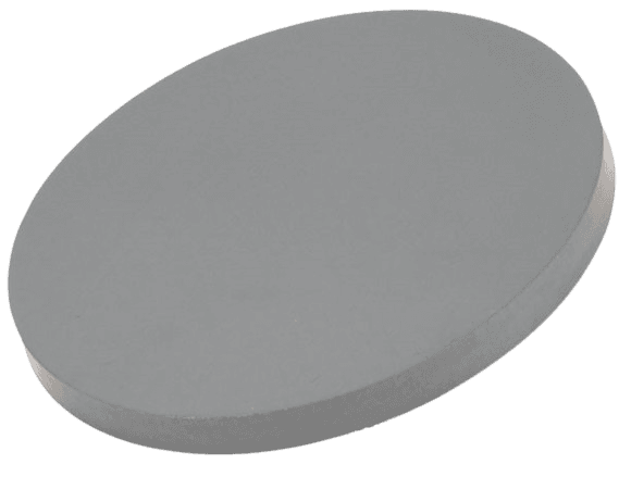
The Indium Tin Oxide (ITO) Sputtering Target is one of the most widely used transparent conductive oxide (TCO) materials for thin film deposition. Composed of indium oxide (In₂O₃) and tin oxide (SnO₂), typically in a 90:10 weight ratio, ITO combines excellent optical transparency with high electrical conductivity. It is indispensable in manufacturing displays, touch panels, solar cells, and optoelectronic devices.
Detailed Description
ITO is a degenerate n-type semiconductor that exhibits both metallic and dielectric properties. Its unique combination of ~85–90% optical transparency and low resistivity (10⁻⁴–10⁻³ Ω·cm) allows it to serve as an electrode material in various optical and electronic devices.
ITO sputtering targets are manufactured through hot pressing, vacuum sintering, or cold isostatic pressing (CIP) to achieve high density and chemical uniformity. The dense structure ensures stable sputtering behavior, low particle generation, and excellent film uniformity on both glass and polymer substrates.
Key Features:
High transparency in visible light and infrared reflection capability.
Low electrical resistivity for efficient current conduction.
Stable film performance under high temperature and plasma conditions.
Custom compositions available (e.g., In₂O₃:SnO₂ = 90:10, 95:5, or 80:20 wt%).
Suitable for both DC and RF magnetron sputtering.
Applications
ITO sputtering targets are used extensively in:
Flat-panel displays (FPD, OLED, LCD) – transparent electrodes.
Touchscreens and smart devices.
Photovoltaic cells – front transparent conductive layers.
Optoelectronic devices – LEDs, sensors, and electrochromic windows.
Architectural and automotive glass coatings – energy-saving low-E films.
Technical Parameters
| Parameter | Typical Value / Range | Importance |
|---|---|---|
| Chemical Formula | (In₂O₃)₁₋ₓ(SnO₂)ₓ | Defines transparency and conductivity |
| Composition Ratio | In₂O₃:SnO₂ = 90:10 wt% | Industry standard for TCO films |
| Purity | 99.9% – 99.99% | Ensures low defect density |
| Density | ≥ 7.0 g/cm³ | Improves sputtering efficiency |
| Resistivity (film) | 10⁻⁴ – 10⁻³ Ω·cm | Provides excellent conductivity |
| Diameter | 25 – 300 mm (custom) | Fits various sputtering systems |
| Thickness | 3 – 10 mm | Balances sputtering lifetime and uniformity |
| Backing Plate | Copper / Titanium | Improves heat dissipation |
Comparison with Related Materials
| Material | Key Advantage | Typical Application |
|---|---|---|
| Indium Tin Oxide (ITO) | Excellent transparency & conductivity | Displays, photovoltaics |
| Aluminum Zinc Oxide (AZO) | Cost-effective TCO alternative | Solar cells |
| Fluorine-doped Tin Oxide (FTO) | High thermal durability | Architectural glass |
| Indium Zinc Oxide (IZO) | Enhanced flexibility & low-temp sputtering | Flexible displays |
FAQ
| Question | Answer |
|---|---|
| Can the In₂O₃:SnO₂ ratio be customized? | Yes, ratios like 95:5 or 80:20 wt% are available upon request. |
| What sputtering systems is ITO compatible with? | Works with both DC and RF magnetron sputtering systems. |
| How is the target bonded? | Typically with copper or titanium backplates for heat management. |
| What’s the typical film transparency? | Over 85% in the visible range. |
| How are the targets packaged? | Vacuum-sealed, foam-cushioned, and packed in export-grade crates. |
Packaging
Each ITO Sputtering Target is vacuum-sealed in moisture-free packaging with desiccants and foam padding. All targets are labeled for traceability and shipped in shockproof, export-safe wooden crates to ensure safe transport.
Conclusion
The Indium Tin Oxide sputtering target is a benchmark material for transparent conductive films, combining superior conductivity, transparency, and process stability. It plays a critical role in modern optoelectronics, offering reliable and customizable performance for both industrial and research applications.
For detailed specifications and quotations, please contact us at [sales@thinfilmmaterials.com].


Reviews
There are no reviews yet.