
 MSDS File
| Material Type | Lead Antimony |
| Symbol | PbSb |
| Melting Point (°C) | N/A |
| Density | N/A |
| Exact Mass | N/A |
| E-Beam | |
| E-Beam Crucible Liner Material | |
| Temp. (°C) for Given Vap. Press. (Torr) | |
| Comments |
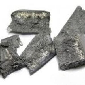
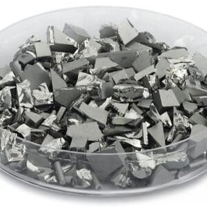
Lead Antimony Pellet Evaporation Material
TFM supplies high-purity Lead Antimony Pellet Evaporation Material, engineered for thin-film deposition in infrared detection, optoelectronics, and advanced semiconductor applications. Composed of lead (Pb) and antimony (Sb), this material features excellent electrical conductivity, strong infrared absorption, and high thermal stability, making it ideal for infrared sensors, photodetectors, and optical coatings.
Designed for thermal evaporation and electron beam (E-beam) evaporation, Lead Antimony Pellet Evaporation Material ensures precise film uniformity, superior adhesion, and exceptional purity, enabling reliable performance in high-tech thin-film applications.
Key Features and Advantages
Superior Infrared Absorption: Perfect for long-wavelength infrared (LWIR) and mid-wavelength infrared (MWIR) detectors.
Optimized Electronic Properties: Supports infrared optoelectronics, photonic devices, and semiconductor applications.
High Purity & Stoichiometric Control: Guarantees consistent thin-film growth for enhanced device efficiency and durability.
Strong Film Adhesion & Uniform Deposition: Ensures reliable and defect-free coatings in optical and electronic applications.
Custom Compositions Available: Tailored to meet specific industry and research needs.
Applications
Infrared Imaging & Thermal Detection: Used in IR cameras, night vision systems, and thermal sensors for defense, aerospace, and industrial applications.
Optoelectronic & Photonic Devices: Plays a crucial role in photoelectric conversion, infrared communication, and high-precision imaging.
Semiconductor & Quantum Research: Supports quantum dot technology, topological insulators, and advanced nanoelectronics.
Thin-Film Coatings for Optical & Electronic Systems: Essential for precision optical coatings and high-sensitivity detection devices.
Industry Impact and Customization
TFM’s Lead Antimony Pellet Evaporation Material is designed to advance infrared detection, optoelectronics, and semiconductor technology. With customizable compositions, precise stoichiometry control, and superior evaporation characteristics, we ensure high-performance thin-film deposition for next-generation infrared and photonic applications.
With its outstanding electronic, optical, and infrared-responsive properties, TFM’s Lead Antimony Pellet Evaporation Material is an essential material for cutting-edge semiconductor innovations, infrared imaging, and high-tech photonic applications, providing enhanced efficiency, stability, and long-term reliability.

Reviews
There are no reviews yet.