Generic selectors
Exact matches only
Search in title
Search in content
Post Type Selectors

ST0025 Lead Sputtering Target, Pb

Chemical Formula: Pb
Catalog Number: ST0025
CAS Number: 7439-92-1
Purity: >99.99%
Shape: Discs, Plates, Column Targets, Step Targets, Custom-made

Lead sputtering target  come in various forms, purities, sizes, and prices. Thin Film Materials (TFM) manufactures and supplies top-quality sputtering targets at competitive prices.

Availability: 1 in stock

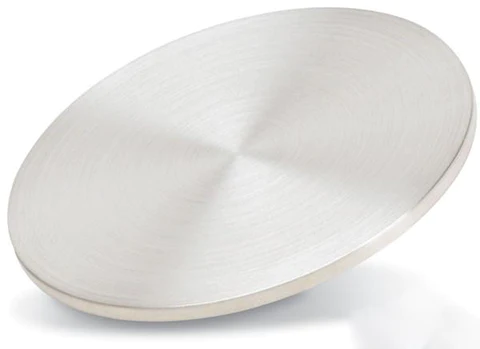
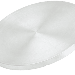
Lead Sputtering Target Description

lead

The lead sputtering target is a bluish-white metallic target made from high-purity lead metal. Lead, also known as plumbum, derives its name from the Anglo-Saxon word “lead” and the Latin “plumbum.” It has been used since 7000 BC, discovered by people from the Near East. The chemical symbol for lead is “Pb,” and it has an atomic number of 82, located in Period 6 and Group 14 of the periodic table, within the p-block. The relative atomic mass of lead is 207.2(1) Dalton, with the number in brackets indicating uncertainty.

Lead Sputtering Target Specification

Material TypeLead
SymbolPb
Color/AppearanceBluish White, Metallic
Melting Point328 °C
Density11.34 g/cc
Thermal Conductivity35 W/m.K
Coefficient of Thermal Expansion28.9 x 10-6/K
Available SizesDia.: 1.0″, 2.0″, 3.0″, 4.0″, 5.0″, 6.0″
Thick: 0.125″, 0.250″

We also offer other customized shapes and sizes of the sputtering targets; please Contact Us for more information.

Lead Sputtering Target Application

The lead sputtering target is used for thin film deposition, decoration, semiconductor, display, LED and photovoltaic devices, functional coating as nicely as other optical information storage space industry, glass coating industry like car glass and architectural glass, optical communication, etc.

Other applications of lead include:

  • Ballasts
  • Counterweights
  • Sound insulation
  • Inertial components
  • In lead-acid batteries
  • Ammunition and armors
  • As a coloring element in ceramic glazes
  • As a protective glass of computer and TV screens to shield the viewer from radiation.

Packaging

Our lead sputter targets are carefully handled to prevent damage during storage and transportation and to preserve the quality of our products in their original condition.

Get Contact

TFM offers Lead Sputtering Targets in various forms, purities, sizes, and prices. We specialize in high-purity thin film deposition materials with optimal density and minimal grain sizes, which are ideal for semiconductor, CVD, and PVD applications in display and optics. Contact Us for current pricing on sputtering targets and other deposition materials that are not listed.

Reviews

There are no reviews yet.

Be the first to review “ST0025 Lead Sputtering Target, Pb”

Your email address will not be published. Required fields are marked *

Related Products

FAQ

It’s the source material (in solid form) used in sputter deposition to eject atoms or molecules that then form a thin film on a substrate.

Targets can be pure metals (e.g., gold, copper, aluminum), ceramics (e.g., Al₂O₃, SiO₂, TiO₂), alloys, or composites—chosen based on the film’s desired properties.


They are produced by processes such as melting/casting for metals or sintering (often with hot isostatic pressing) for ceramics and composite targets to ensure high density and purity.


In a vacuum chamber, a plasma (typically argon) bombards the target, ejecting atoms that travel and condense on a substrate, forming a thin film.


Key factors include the target’s purity, density, grain structure, and the sputtering yield (i.e. how many atoms are ejected per incident ion), as well as operating conditions like power density and gas pressure.


Operators monitor target erosion (often by measuring the depth of the eroded “race track”) or track total energy delivered (kilowatt-hours) until it reaches a threshold that can compromise film quality.


Fragile materials (such as many ceramics or certain oxides) and precious metals often require a backing plate to improve cooling, mechanical stability, and to allow thinner targets that reduce material costs.


DC sputtering is used for conductive targets, while RF sputtering is necessary for insulating targets (like many oxides) because it prevents charge buildup on the target’s surface.


In reactive sputtering, a reactive gas (e.g., oxygen or nitrogen) is introduced to form compound films on the substrate, but it may also “poison” the target surface if not carefully controlled.


Many manufacturers prefer to control raw material quality by sourcing their own powders; using external powders can risk impurities and inconsistent target properties.


Targets should be stored in clean, dry conditions (often in original packaging or re-wrapped in protective materials) and handled with gloves to avoid contamination, ensuring optimal performance during deposition.

Deposition rate depends on factors such as target material and composition, power density, working gas pressure, substrate distance, and the configuration of the sputtering system (e.g., magnetron design).

 
Shopping Cart
Scroll to Top