 MSDS File
Introduction
Magnesium Silicide Evaporation Materials (Mg₂Si) are compound semiconductor materials used in thin film deposition processes for thermoelectric devices, semiconductor research, and advanced energy applications. Magnesium silicide is an environmentally friendly semiconductor composed of abundant elements, making it attractive for sustainable electronic and thermoelectric technologies.
When used in physical vapor deposition (PVD) processes such as thermal evaporation or electron beam evaporation, Mg₂Si evaporation materials enable the deposition of thin films with controlled composition and uniform structure. These films are widely studied for thermoelectric power generation, infrared sensing, and semiconductor device development.
Detailed Description
Magnesium silicide evaporation materials are produced by synthesizing high-purity magnesium and silicon under controlled conditions to form the Mg₂Si compound. Manufacturing processes typically include vacuum melting, powder metallurgy, or solid-state reactions followed by sintering. These methods ensure a homogeneous material composition and stable evaporation behavior.
Mg₂Si is a semiconductor material with a narrow bandgap and excellent thermoelectric properties. It has attracted considerable attention as a candidate material for mid-temperature thermoelectric generators, where waste heat can be converted into electrical energy. Compared with many traditional thermoelectric materials, magnesium silicide offers advantages such as low toxicity, relatively low density, and good thermal stability.
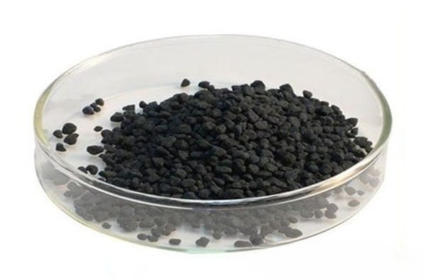
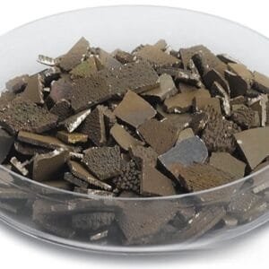
In evaporation deposition systems, Mg₂Si materials are typically supplied as pellets, granules, tablets, or pieces designed for electron beam or resistive heating sources. The uniform composition of the evaporation material ensures stable vaporization and consistent thin film composition during deposition.
Thin films deposited from Mg₂Si evaporation materials can exhibit useful electrical and thermoelectric characteristics, making them valuable in experimental semiconductor structures and energy conversion technologies.
Applications
Magnesium Silicide evaporation materials are used in several advanced technology and research fields:
Thermoelectric materials used for waste heat recovery and power generation
Semiconductor thin film research involving silicide-based compounds
Infrared sensing materials in optoelectronic devices
Energy conversion technologies using thermoelectric modules
Thin film electronics requiring semiconductor silicide layers
Academic and industrial research laboratories studying sustainable semiconductor materials
Technical Parameters
| Parameter | Typical Value / Range | Importance |
|---|---|---|
| Purity | 99.9% – 99.99% | High purity improves semiconductor performance |
| Chemical Formula | Mg₂Si | Determines electrical and thermoelectric properties |
| Form | Pellets / Granules / Tablets | Suitable for evaporation sources |
| Particle Size | 1 – 6 mm typical | Ensures stable evaporation rates |
| Density | High-density sintered material | Provides consistent deposition behavior |
| Deposition Method | E-beam evaporation / Thermal evaporation | Compatible with PVD thin film processes |
Comparison with Related Materials
| Material | Key Advantage | Typical Application |
|---|---|---|
| Magnesium Silicide (Mg₂Si) | Environmentally friendly thermoelectric semiconductor | Waste heat recovery and thermoelectric devices |
| Bismuth Telluride (Bi₂Te₃) | High thermoelectric efficiency near room temperature | Thermoelectric cooling and power generation |
| Silicon (Si) | Widely used semiconductor material | Electronics and microchips |
FAQ
| Question | Answer |
|---|---|
| What forms are available for Mg₂Si evaporation materials? | They are typically supplied as pellets, granules, tablets, or pieces suitable for evaporation sources. |
| Which deposition methods are compatible with Mg₂Si? | Mg₂Si materials are commonly used in electron beam evaporation and thermal evaporation systems. |
| What purity levels are available? | Standard purity ranges from 99.9% to 99.99%, depending on application requirements. |
| What substrates can Mg₂Si films be deposited on? | Mg₂Si films can be deposited on silicon wafers, glass, ceramic substrates, and other semiconductor materials. |
| What industries use Mg₂Si materials most frequently? | Thermoelectric device development, semiconductor research, and advanced energy technology industries. |
Packaging
Our Magnesium Silicide Evaporation Materials (Mg₂Si) are meticulously tagged and labeled externally to ensure efficient identification and maintain high standards of quality control. The materials are packaged in vacuum-sealed bags or inert atmosphere containers to prevent oxidation and contamination. Protective cushioning and export-grade cartons or wooden crates are used to ensure safe storage and transportation.
Conclusion
Magnesium Silicide Evaporation Materials (Mg₂Si) provide a promising material solution for thin film deposition in thermoelectric energy systems and semiconductor research. Their environmentally friendly composition, semiconductor characteristics, and compatibility with evaporation processes make them suitable for next-generation energy and electronic technologies.
With customizable forms, high purity levels, and stable evaporation performance, Mg₂Si evaporation materials support advanced thin film deposition and sustainable materials research.
For detailed specifications and a quotation, please contact us at sales@thinfilmmaterials.com.


Reviews
There are no reviews yet.