 MSDS File
Manganese(II) Sulfide Evaporation Materials Overview
Our manganese(II) sulfide evaporation material, provided by TFM, is a premium ceramic material with the chemical formula MnS. This high-purity material is essential for achieving top-notch film quality in various deposition processes. TFM ensures a purity level of up to 99.9995% through rigorous quality assurance measures, guaranteeing reliable performance.
Specifications
| Material Type | Manganese(II) sulfide |
| Symbol | MnS |
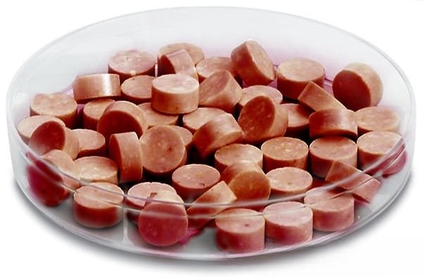
| Appearance/Color | Red, green or brown solid |
| Melting Point | 1610 ˚C |
| Density | 3.99 g/cm |
| Purity | 99.9% |
| Shape | Powder/ Granule/ Custom-made |
Applications
Manganese(II) sulfide evaporation materials are used in various deposition techniques, including:
- Semiconductor Deposition
- Chemical Vapor Deposition (CVD)
- Physical Vapor Deposition (PVD)
These materials are particularly suited for optical applications, including protective coatings, decorative finishes, and display technologies.
Packaging
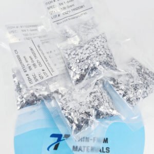
We ensure that manganese(II) sulfide evaporation materials are meticulously packaged with clear labels for easy identification and quality control. Our packaging process is designed to prevent any damage during storage and transportation.
Contact Us
TFM is a leading supplier of high-purity manganese(II) sulfide evaporation materials, available in multiple forms such as tablets, granules, rods, and wires. Custom options are also available. In addition to evaporation materials, we offer evaporation sources, boats, filaments, crucibles, heaters, and e-beam crucible liners. For current pricing and inquiries about materials not listed, please contact us directly.


Reviews
There are no reviews yet.