
Molybdenum Boride Sputtering Target Description
Molybdenum Boride Sputtering Target is used in the sputtering process, a technique for depositing thin films onto substrates. In this process, high-energy ions bombard the target material, causing atoms or molecules to be ejected from the target surface. These ejected particles then deposit onto a substrate, forming a thin film.
Molybdenum Boride Sputtering Targets are commonly used to produce coatings that improve wear resistance, enhance surface durability, and provide specific optical or electrical properties.
Related Product: Molybdenum Boride Sputtering Target (Mo2B5)
Molybdenum Boride Sputtering Target Specifications
| Compound Formula | Mo2B |
| Molecular Weight | 202.69 |
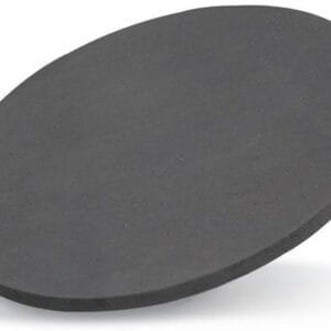
| Appearance | Gray target |
| Melting Point | 2000 |
| Density (g/cm3) | 9.2 |
| Available Sizes | Dia.: 1.0″, 2.0″, 3.0″, 4.0″, 5.0″, 6.0″ Thick: 0.125″, 0.250″ |
Molybdenum Boride Sputtering Target Handling Notes
Indium bonding is recommended for the Molybdenum Boride Sputtering Target due to its characteristics that are not amenable to sputtering, such as brittleness and low thermal conductivity. This material has low thermal conductivity and is susceptible to thermal shock, which makes indium bonding a suitable choice to ensure stability and performance during the sputtering process.
Molybdenum Boride Sputtering Target Application
The Molybdenum Boride Sputtering Target is widely used in the production of coatings for tools, electronic devices, and other surfaces where its specific properties, such as enhanced wear resistance and hardness, are desirable.
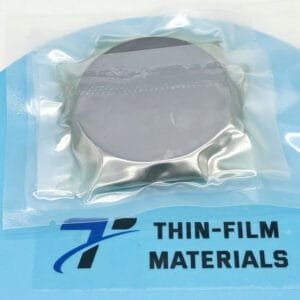
Molybdenum Boride Sputtering Target Packaging
Our Molybdenum Boride Sputtering Target is widely utilized in the production of coatings for various applications. These include improving the wear resistance of tools, enhancing the durability of surfaces, and providing specific optical or electrical properties.
Get Contact
TFM offers Molybdenum Boride Sputtering Targets in various forms, purities, sizes, and prices. We specialize in high-purity thin film deposition materials with optimal density and minimal grain sizes, which are ideal for semiconductor, CVD, and PVD applications in display and optics. Contact Us for current pricing on sputtering targets and other deposition materials that are not listed.

Reviews
There are no reviews yet.