 MSDS File
Introduction
Molybdenum Diselenide (MoSe₂) Evaporation Materials are widely used in advanced thin film deposition processes for electronics, optoelectronics, and two-dimensional (2D) materials research. As a member of the transition metal dichalcogenide (TMD) family, MoSe₂ exhibits unique layered structures, tunable electronic properties, and excellent optical characteristics.
These materials are commonly used in Physical Vapor Deposition (PVD) techniques such as thermal evaporation and electron beam evaporation to fabricate high-quality thin films and layered structures. MoSe₂ evaporation materials are particularly valuable in research areas related to nanoelectronics, flexible electronics, and next-generation semiconductor technologies.
Detailed Description
Molybdenum Diselenide (MoSe₂) is a layered compound consisting of molybdenum atoms sandwiched between two layers of selenium atoms, forming a Se–Mo–Se structure. This layered arrangement is characterized by strong covalent bonding within each layer and weak van der Waals interactions between layers. As a result, MoSe₂ can form atomically thin layers and exhibits unique electronic and optical properties.
MoSe₂ belongs to the broader class of transition metal dichalcogenides that have attracted significant attention in recent years due to their potential use in two-dimensional electronics and optoelectronic devices. In monolayer or few-layer form, MoSe₂ behaves as a semiconductor with a direct bandgap, which is particularly useful for optoelectronic applications such as photodetectors and light-emitting devices.
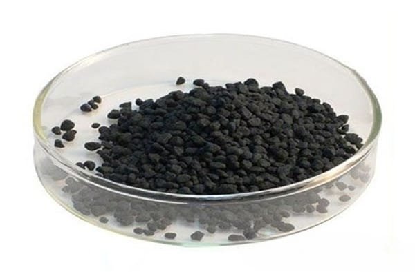
When used as evaporation materials in vacuum deposition systems, MoSe₂ is typically supplied in the form of granules, pellets, or pieces suitable for loading into evaporation sources such as crucibles or boats. High-purity materials ensure stable evaporation behavior and accurate stoichiometry in the resulting thin films.
During the evaporation process, MoSe₂ material vaporizes under high vacuum and condenses onto substrates to form thin films. The deposition conditions—such as substrate temperature, vacuum level, and deposition rate—can influence the crystallinity, thickness, and morphology of the resulting film.
MoSe₂ thin films are widely studied for their electronic transport properties, optical absorption, and catalytic activity. In addition, the material’s compatibility with layered heterostructures allows it to be integrated with other two-dimensional materials such as graphene or tungsten diselenide, enabling the fabrication of advanced electronic devices.
Applications
Molybdenum Diselenide evaporation materials are used in a variety of emerging technologies and research areas, including:
Two-dimensional semiconductor materials research
Nanoelectronic and optoelectronic devices
Photodetectors and light-emitting devices
Layered van der Waals heterostructures
Catalytic materials for hydrogen evolution reactions (HER)
Flexible and wearable electronic devices
Because of its tunable bandgap and layered structure, MoSe₂ is considered a promising material for future semiconductor technologies.
Technical Parameters
| Parameter | Typical Value / Range | Importance |
|---|---|---|
| Purity | 99.9% – 99.999% | Ensures high-quality thin film deposition |
| Chemical Formula | MoSe₂ | Maintains correct compound stoichiometry |
| Density | ~6.0 g/cm³ | Influences evaporation behavior |
| Melting Point | ~1200 °C (decomposition region) | Determines evaporation conditions |
| Form | Granules / Pellets / Pieces | Compatible with evaporation sources |
| Deposition Method | Thermal / E-Beam Evaporation | Suitable for common PVD systems |
Comparison with Related Materials
| Material | Key Advantage | Typical Application |
|---|---|---|
| Molybdenum Diselenide (MoSe₂) | Direct bandgap in monolayer form | Optoelectronic and nanoelectronic devices |
| Molybdenum Disulfide (MoS₂) | Widely studied 2D semiconductor | Transistors and sensors |
| Tungsten Diselenide (WSe₂) | Excellent optical properties | Photodetectors and LEDs |
| Niobium Diselenide (NbSe₂) | Superconductivity and metallic conductivity | Quantum materials research |
FAQ
| Question | Answer |
|---|---|
| What deposition methods can use MoSe₂ evaporation materials? | They are typically used in thermal evaporation or electron beam evaporation systems. |
| Why is MoSe₂ important for 2D materials research? | MoSe₂ exhibits tunable electronic and optical properties and can form atomically thin semiconductor layers. |
| What substrates are commonly used for MoSe₂ thin films? | Silicon wafers, sapphire, glass, and other 2D material substrates are commonly used. |
| Can the evaporation materials be customized? | Yes, purity level, particle size, and packaging can be customized to fit specific deposition systems. |
| Are MoSe₂ films suitable for optoelectronic devices? | Yes, monolayer MoSe₂ has a direct bandgap that is useful for photodetectors and other optoelectronic applications. |
Packaging
Our Molybdenum Diselenide Evaporation Materials are meticulously tagged and labeled externally to ensure efficient identification and maintain high standards of quality control. We take great care to prevent any potential damage during storage and transportation, ensuring the targets arrive in perfect condition.
Conclusion
Molybdenum Diselenide (MoSe₂) evaporation materials provide a reliable source for producing high-quality transition metal dichalcogenide thin films with unique electronic and optical properties. Their layered crystal structure and semiconductor behavior make them highly valuable in next-generation electronics, optoelectronics, and two-dimensional materials research.
With customizable purity levels, particle sizes, and packaging options, MoSe₂ evaporation materials are suitable for both advanced research applications and thin film deposition systems.
For detailed specifications and a quotation, please contact us at sales@thinfilmmaterials.com.


Reviews
There are no reviews yet.