
 MSDS File
Molybdenum Disilicide Evaporation Materials Overview
Molybdenum disilicide (MoSi₂) is a high-performance ceramic evaporation material renowned for its critical role in achieving superior deposition results. At TFM, we provide molybdenum disilicide evaporation materials with exceptional purity levels, up to 99.9995%, ensuring the highest quality films in your deposition processes.
Molybdenum Disilicide Evaporation Materials Specification
| Material Type | Molybdenum Disilicide |
| Symbol | MoSi2 |
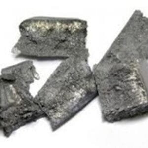
| Appearance/Color | Gray metallic solid |
| Melting Point | 2,030 °C (3,690 °F; 2,300 K) |
| Density | 6.26 g/cm3 |
| Purity | 99.5% |
| Shape | Powder/ Granule/ Custom-made |
Applications
Our molybdenum disilicide evaporation materials are essential in various deposition techniques, including:
- Semiconductor Deposition
- Chemical Vapor Deposition (CVD)
- Physical Vapor Deposition (PVD)
They are widely used in optics for applications such as wear protection, decorative coatings, and display technologies.
Packaging and Quality Assurance
Each batch of molybdenum disilicide evaporation material is carefully tagged and labeled to facilitate efficient identification and maintain rigorous quality control standards. We prioritize protecting the materials during storage and transportation to avoid any damage.
Contact Us
TFM stands as a premier provider of high-purity molybdenum disilicide evaporation materials. We offer various shapes including tablets, granules, rods, and wires, with custom forms and quantities available upon request. Additionally, we supply a range of evaporation sources, boats, filaments, crucibles, heaters, and e-beam crucible liners. For current pricing and additional information, please contact us with your inquiry.


Reviews
There are no reviews yet.