Generic selectors
Exact matches only
Search in title
Search in content
Post Type Selectors

VD0823 Molybdenum Disulfide Evaporation Materials, MoS2

Catalog No.VD0823
MaterialMolybdenum Disulfide (MoS2)
Purity99%
ShapePowder/ Granule/ Custom-made

TFM stands out as a top-tier manufacturer and supplier specializing in high-purity molybdenum disulfide (MoS₂) evaporation materials. Our commitment to quality and precision ensures that our products meet the highest standards, making us the go-to choice for industries requiring reliable and high-performance evaporation materials.

Molybdenum Disulfide Evaporation Materials Overview

Molybdenum disulfide (MoS2) evaporation materials, supplied by TFM, are high-purity ceramic compounds crucial for various deposition techniques. MoS2 is known for its ability to produce high-quality thin films, making it essential in semiconductor, chemical vapor deposition (CVD), and physical vapor deposition (PVD) processes. TFM’s MoS2 materials are available with purity levels reaching up to 99.9995%, ensuring exceptional performance and reliability.

Specifications of Molybdenum Disulfide Evaporation Materials

Material TypeMolybdenum Disulfide
SymbolMoS2
Appearance/ColorBlack/lead-gray solid
Melting Point2,375 °C (4,307 °F; 2,648 K)
Density5.06 g/cm3
Purity99%
ShapePowder/ Granule/ Custom-made

Applications of Molybdenum Disulfide Evaporation Materials

MoS2 evaporation materials are widely utilized in various deposition processes. These include:

  • Semiconductor Deposition
  • Chemical Vapor Deposition (CVD)
  • Physical Vapor Deposition (PVD)

They are predominantly used in applications such as:

  • Optical Coatings
  • Wear Protection
  • Decorative Coatings
  • Display Technologies

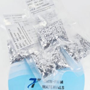
Packaging and Handling

TFM ensures that molybdenum disulfide evaporation materials are meticulously packaged and labeled for easy identification and quality control. The packaging is designed to prevent damage during storage and transport, maintaining the integrity of the materials.

Contact Us

TFM is a premier manufacturer and supplier of high-purity molybdenum disulfide evaporation materials. We offer a range of forms, including tablets, granules, rods, and wires, and can provide custom solutions upon request. We also supply evaporation sources, boats, filaments, crucibles, heaters, and e-beam crucible liners. For current pricing and inquiries regarding products not listed, please contact us directly.

Reviews

There are no reviews yet.

Be the first to review “VD0823 Molybdenum Disulfide Evaporation Materials, MoS2”

Your email address will not be published. Required fields are marked *

FAQ

  • They are high‐purity substances (e.g. metals, alloys, or compounds) used in thermal or electron‐beam evaporation processes to form thin films on substrates.

  • Typically, they’re processed into a form (often ingots, pellets, or wires) that can be efficiently vaporized. Preparation emphasizes high purity and controlled composition to ensure film quality.

  • Thermal evaporation and electron-beam (e-beam) evaporation are the two main techniques, where material is heated (or bombarded with electrons) until it vaporizes and then condenses on the substrate.

  • Thermal evaporation heats the material directly (often using a resistive heater), while e-beam evaporation uses a focused electron beam to locally heat and vaporize the source material—each method offering different control and energy efficiency.

  • Key parameters include source temperature, vacuum level, deposition rate, substrate temperature, and the distance between the source and the substrate. These factors influence film uniformity, adhesion, and microstructure.

  • Evaporation generally produces high-purity films with excellent control over thickness, and it is especially suitable for materials with relatively low melting points or high vapor pressures.

  • Challenges include issues with step coverage (due to line-of-sight deposition), shadowing effects on complex topographies, and possible re-evaporation of material from the substrate if temperature isn’t properly controlled.

  • Common evaporation materials include noble metals (e.g., gold, silver), semiconductors (e.g., silicon, germanium), metal oxides, and organic compounds—each chosen for its specific optical, electrical, or mechanical properties.

  • Selection depends on desired film properties (conductivity, optical transparency, adhesion), compatibility with the evaporation process, and the final device application (semiconductor, optical coating, etc.).

  • Optimizing substrate temperature, deposition rate, and chamber vacuum are critical for ensuring that the film adheres well and forms the intended microstructure without defects.

  • Troubleshooting may involve checking the source material’s purity, ensuring stable source temperature, verifying the vacuum level, adjusting the substrate’s position or temperature, and monitoring deposition rate fluctuations.

While evaporation tends to yield very high purity films with excellent thickness control, it is limited by its line-of-sight nature. In contrast, sputtering can deposit films more uniformly on complex surfaces and is more versatile for a broader range of materials.


Shopping Cart
Scroll to Top