 MSDS File
Introduction
Molybdenum Evaporation Materials (Mo) are widely used in vacuum deposition processes where thermal stability, controlled vaporization behavior, and strong adhesion to substrates are required. As a refractory metal with a high melting point and low vapor pressure under high vacuum, molybdenum is particularly suitable for electron beam evaporation and high-temperature coating systems.
Mo thin films are valued for their electrical conductivity, thermal stability, and mechanical strength, making them essential in semiconductor devices, thin film photovoltaics, display technology, and advanced research applications.
Detailed Description
Molybdenum (Mo) has a melting point of approximately 2623 °C and excellent dimensional stability at elevated temperatures. Evaporation materials are typically produced from high-purity molybdenum ingots through vacuum melting and precision machining to ensure chemical uniformity and low impurity levels.
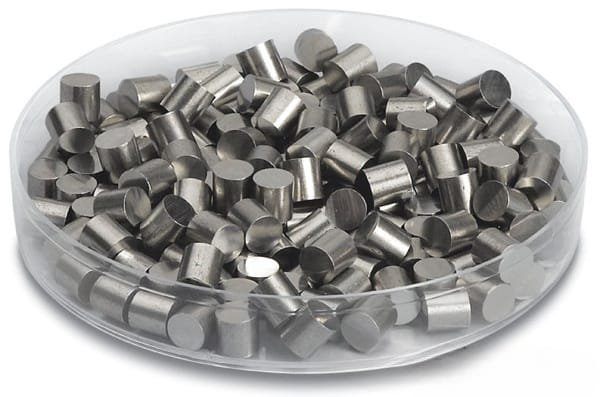
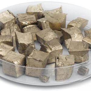
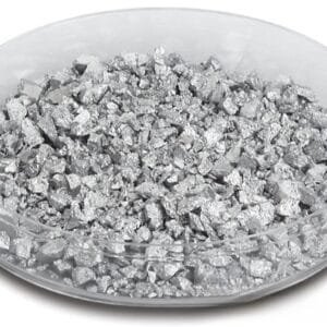
Available forms include:
Pellets
Granules
Rods or slugs
Custom-cut pieces
High purity grades (typically 99.9% – 99.99%) minimize contamination during thin film growth. Controlled surface finishing reduces oxide contamination and improves evaporation stability.
Key material characteristics include:
High melting point suitable for e-beam evaporation
Excellent electrical conductivity
Strong adhesion to glass, silicon, and oxide substrates
Low coefficient of thermal expansion compared to many metals
Good compatibility with multilayer stacks
Molybdenum evaporation materials are most commonly used in electron beam evaporation systems due to their refractory nature. Thermal evaporation is possible but requires robust heating sources.
Applications
Molybdenum Evaporation Materials are widely applied in:
Semiconductor metallization layers
Thin film solar cells (CIGS back contacts)
Display technologies (TFT electrodes)
Diffusion barrier and adhesion layers
Optical coatings requiring stable metallic layers
Microelectromechanical systems (MEMS)
Research in refractory metal thin films
In CIGS photovoltaic cells, molybdenum films serve as the standard back contact layer due to their conductivity and chemical compatibility with absorber layers.
Technical Parameters
| Parameter | Typical Value / Range | Importance |
|---|---|---|
| Chemical Symbol | Mo | Defines refractory metal characteristics |
| Purity | 99.9% – 99.99% | Reduces contamination in thin films |
| Form | Pellets / Granules / Slugs | Compatible with various crucibles |
| Size | Custom (1–20 mm typical pieces) | Matches evaporation source design |
| Melting Point | ~2623 °C | Determines suitable deposition method |
| Density | ~10.2 g/cm³ | Relevant for deposition rate calculation |
Custom geometries can be provided to match specific evaporation boats or crucibles.
Comparison with Related Refractory Metals
| Material | Key Advantage | Typical Application |
|---|---|---|
| Molybdenum (Mo) | Balanced conductivity & thermal stability | Solar back contacts & electrodes |
| Tungsten (W) | Higher melting point | Extreme temperature environments |
| Tantalum (Ta) | Excellent corrosion resistance | Chemical processing & electronics |
| Chromium (Cr) | Strong adhesion & hardness | Adhesion layers |
Compared with tungsten, molybdenum offers easier processing and lower density while still maintaining excellent high-temperature performance.
FAQ
| Question | Answer |
|---|---|
| Is Mo suitable for thermal evaporation? | It can be used, but electron beam evaporation is typically preferred due to its high melting point. |
| Can the material be customized in size? | Yes, pellets, granules, and custom shapes are available. |
| Is molybdenum prone to oxidation? | Surface oxidation may occur; storage in dry or inert conditions is recommended. |
| Is it compatible with semiconductor processes? | Yes, it is widely used in semiconductor and photovoltaic manufacturing. |
| Are certificates provided? | Yes, material certification and batch traceability are available upon request. |
Packaging
Our Molybdenum Evaporation Materials are meticulously tagged and labeled externally to ensure efficient identification and maintain high standards of quality control. We take great care to prevent any potential damage during storage and transportation, ensuring the materials arrive in perfect condition.
Conclusion
Molybdenum Evaporation Materials (Mo) provide a stable and reliable solution for high-temperature vacuum deposition processes. With controlled purity, consistent evaporation behavior, and flexible customization options, they support advanced semiconductor, photovoltaic, and research applications.
For detailed specifications and a quotation, please contact us at sales@thinfilmmaterials.com.
Ordering Table
| Material | Size | Quantity | Purity | Notes | Part Number |
| Molybdenum | 1/4" Dia. x 1/2" Length | 1 lb. | 99.95% | — | EVMMO35QXH |
| Molybdenum | 1/4" Dia. x 1/4" Length | 1 lb. | 99.95% | — | EVMMO35QXQ |
| Molybdenum | 1/4" Dia. x 1/4" Length | 25 g | 99.95% | — | EVMMO35QXQA |
| Molybdenum | 1/4" Dia. x 1/4" Length | 50 g | 99.95% | — | EVMMO35QXQB |
| Molybdenum | 1/4" Dia. x 1/4" Length | 100 g | 99.95% | — | EVMMO35QXQD |
| Molybdenum | 1/8" Dia. x 1/4" Length | 1 lb. | 99.95% | — | EVMMO35EXQ |
| Molybdenum | 1/8" Dia. x 1/8" Length | 1 lb. | 99.95% | — | EVMMO35EXE |
| Molybdenum | 1/8" Dia. x 1/8" Length | 100 g | 99.95% | — | EVMMO35EXED |
| Molybdenum | 1/8" Dia. x 1/8" Length | 250 g | 99.95% | — | EVMMO35EXEJ |
| Molybdenum | Approx. 1/4" x 1/4" Pieces | Per Gram | 99.95% | EVMMO35SPL10 |

Reviews
There are no reviews yet.