 MSDS File
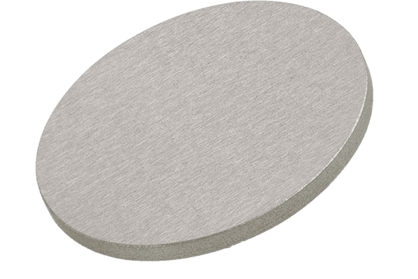
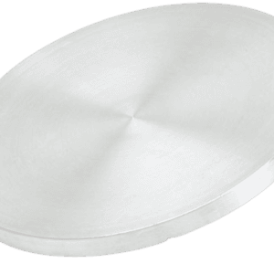
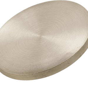
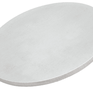
Molybdenum Silicon Sputtering Target Description
Molybdenum Silicon Sputtering Targets are highly valued in advanced technology sectors due to their distinctive attributes. Their superior electrical conductivity makes them well-suited for use in electronic devices, delivering exceptional performance in semiconductor applications. Additionally, these targets are noted for their impressive thermal stability, enabling them to perform reliably even in high-temperature conditions, which is crucial for the production of electronic components.
In the realm of optoelectronics, Molybdenum Silicon Sputtering Targets stand out due to their specialized optical characteristics. They are particularly effective in applications involving laser devices and photodetectors. The targets also demonstrate excellent chemical stability, which allows them to maintain their performance and reliability in complex manufacturing environments. This makes them a dependable choice for various high-tech applications.
Related Product: Aluminum Silicon Copper Sputtering Target, Aluminum Silicon Sputtering Target
Molybdenum Silicon Sputtering Target Specifications
| Compound Formula | MoSi |
| Molecular Weight | 124.035 |
| Appearance | Silver Metallic Target |
| Melting Point | 2077 °C |
| Available Sizes | Dia.: 1.0″, 2.0″, 3.0″, 4.0″, 5.0″, 6.0″
Thick: 0.125″, 0.250″ |
Molybdenum Silicon Sputtering Target Handling Notes
Indium bonding is highly recommended for Molybdenum Silicon Sputtering Targets due to certain material characteristics that can complicate traditional sputtering processes. Molybdenum Silicon exhibits brittleness and low thermal conductivity, making it prone to thermal shock and potential performance issues during sputtering. Using Indium bonding helps to address these challenges by providing a more stable and effective attachment, thereby ensuring improved durability and consistent performance of the sputtering targets under operational conditions.
Molybdenum Silicon Sputtering Target Application
Molybdenum Silicon Sputtering Targets are highly valued across a range of high-tech applications due to their exceptional properties. In electronic device manufacturing, these targets are prized for their excellent electrical conductivity, making them essential for producing high-performance components such as semiconductors, transistors, and integrated circuits. Their role extends into optoelectronics as well, where their optical properties make them well-suited for laser devices and photodetectors, supporting advancements in laser technology and optical communications.
Additionally, Molybdenum Silicon Sputtering Targets contribute to the efficiency of solar cell production. Their combination of electrical and optical properties enhances solar energy conversion, making them a crucial component in the development of advanced solar technologies.
Molybdenum Silicon Sputtering Target Packaging
We ensure that our Molybdenum Silicon Sputtering Targets are meticulously handled during both storage and transportation to maintain their quality and integrity.
Get Contact
TFM’s Molybdenum Silicon Sputtering Targets are offered in a range of forms, purities, and sizes. We focus on producing high-purity physical vapor deposition (PVD) materials with optimal density and the smallest average grain sizes, tailored for applications in semiconductor manufacturing, chemical vapor deposition (CVD), and physical vapor deposition (PVD) for display and optical uses.
Reviews
There are no reviews yet.