
Product Overview
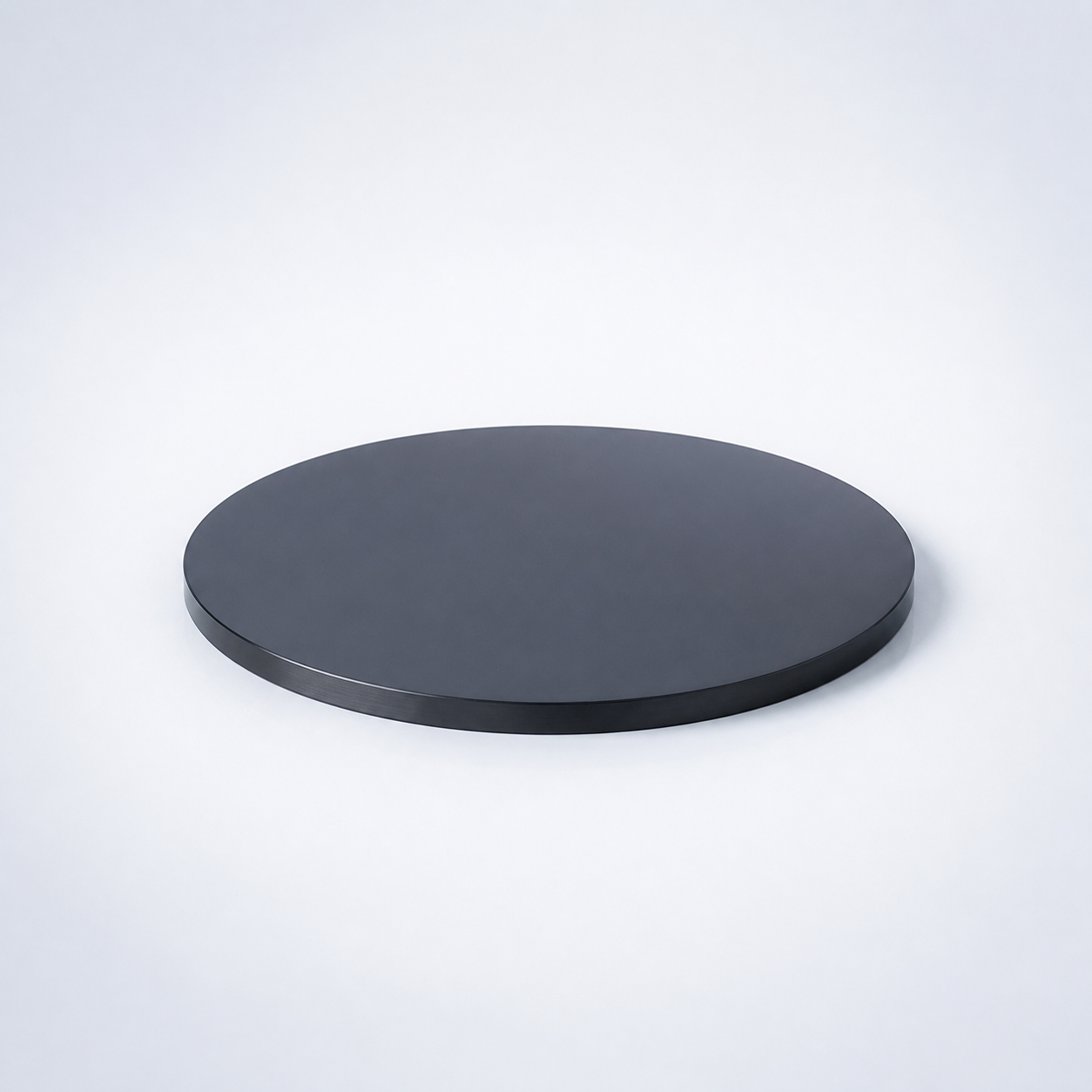
N-type Silicon Sputtering Target (N-doped Si) (N-doped Si) is a composition-specific sputtering target for thin-film deposition and PVD process development. The practical specification normally includes chemistry, purity, dimensions, density, target configuration, and any bonding or backing requirement needed by the sputtering cathode.
Material and Deposition Characteristics
Power mode and process conditions should be selected according to the target conductivity, thermal behavior, and the requirements of the cathode system. For less common materials, conservative initial power density and film-composition verification are good practice.
Technical Data
| Parameter | Typical Value / Range | Importance |
|---|---|---|
| Purity | 99.999% (5N) typical | High purity ensures semiconductor-grade film quality |
| Dopant Type | P / As / Sb | Determines electrical conductivity |
| Resistivity | Custom range (e.g., 0.001–10 Ω·cm) | Controls carrier concentration |
| Diameter | 25 – 300 mm (custom) | Compatible with various sputtering systems |
| Thickness | 3 – 10 mm | Influences sputtering rate and target lifetime |
| Bonding | Copper backing plate (optional) | Improves heat transfer and structural stability |
| Material | Key Advantage | Typical Application |
|---|---|---|
| N-type Silicon (N-doped Si) | High electron conductivity | Semiconductor devices and photovoltaic layers |
| P-type Silicon | Hole conductivity | Complementary semiconductor structures |
| Undoped Silicon | High purity but low conductivity | Research and insulating layers |
| Question | Answer |
|---|---|
| What does N-type silicon mean? | N-type silicon contains donor dopants such as phosphorus or arsenic that introduce extra electrons, increasing electrical conductivity. |
| Why is doping required for sputtering targets? | Doping improves electrical conductivity, allowing the target to be used in DC magnetron sputtering systems. |
| Can the resistivity be customized? | Yes, dopant concentration can be adjusted to achieve specific resistivity levels required by semiconductor processes. |
| Are bonded targets available? | Yes, N-type silicon targets can be bonded to copper backing plates for improved thermal management during sputtering. |
| Which industries use N-type silicon sputtering targets? | Semiconductor manufacturing, solar cell production, display technologies, and advanced electronics research laboratories. |
Typical Thin-Film Applications
- Thin-film research and materials-development projects requiring a composition-specific sputtering source
- Semiconductor, optical, energy, electronic, or laboratory coatings depending on the material system
- Custom R&D work where target composition, purity, and geometry need to be specified together
Target Configuration and Ordering Considerations
For quotation and manufacturability review, provide target size, thickness, purity or alloy composition, quantity, and the sputtering gun or cathode model if known. If a bonded assembly is required, include backing-plate material, bonding preference, and any dimensional tolerances, surface-finish needs, or inspection-document requirements. TFM can also review customer drawings or old-target samples for replacement builds.
Frequently Asked Questions
What is the main reason to use a N-type Silicon (N-doped Si) sputtering target?
It provides a composition-specific source for thin-film deposition when the target material itself is important to the desired film chemistry or process.
How should the sputtering mode for N-type Silicon (N-doped Si) be selected?
The power mode should be chosen according to target conductivity, thermal behavior, and equipment capability. Less-conductive materials are commonly evaluated with RF power.
Why are density and microstructure important for N-type Silicon (N-doped Si) targets?
These factors can influence erosion stability, thermal behavior, particle generation, and the risk of cracking or local hot spots.
Can N-type Silicon (N-doped Si) be supplied with a backing plate?
Yes. If the material is brittle or the cathode requires it, a bonded configuration can be reviewed according to target size, thickness, cooling, and power.
Does target composition always equal film composition?
No. Film chemistry may differ because of sputtering yields, process conditions, substrate temperature, re-sputtering, and chamber history. Film verification is recommended when composition matters.
What should I provide to request a quotation for N-type Silicon (N-doped Si)?
Please provide the composition, purity, dimensions, quantity, target configuration, cathode details, and any drawing or inspection requirements.

Reviews
There are no reviews yet.