Generic selectors
Exact matches only
Search in title
Search in content
Post Type Selectors

VD0837 Nickel Boride Evaporation Materials, Ni2B

Catalog No.VD0837
MaterialNickel boride (Ni2B)
Purity99.5%
ShapePowder/ Granule/ Custom-made

TFM is at the forefront of producing and supplying top-quality nickel boride evaporation materials, known for their high purity and reliability. Our extensive product range includes both powder and granule forms of evaporation materials, with options for custom forms available upon request. Whether you need standard or bespoke solutions, TFM is dedicated to meeting your specific requirements with precision and expertise.

Nickel Boride Evaporation Materials Overview

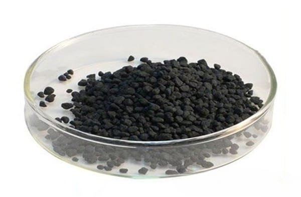
Nickel boride evaporation materials, identified by the chemical formula Ni2B, are crucial for achieving high-quality deposition films. TFM specializes in delivering nickel boride with exceptional purity levels of up to 99.9995%, ensured through stringent quality control measures.

Product Specifications

Material TypeNickel Boride
SymbolNi2B
Appearance/ColorSolid
Melting Point~ 1125 °C (2057 °F)
Density7.9 g/cm3
Purity99.5%
ShapePowder/ Granule/ Custom-made

Applications

Nickel boride evaporation materials are utilized in a range of deposition techniques, such as:

  • Semiconductor Deposition
  • Chemical Vapor Deposition (CVD)
  • Physical Vapor Deposition (PVD)

These materials are particularly effective in optics applications, including wear protection, decorative coatings, and display enhancements.

Packaging and Handling

To ensure efficient identification and quality control, our nickel boride evaporation materials are meticulously tagged and labeled. We take great care to prevent any damage during storage and transportation.

Contact Us

TFM provides nickel boride evaporation materials in various shapes, including tablets, granules, rods, and wires, with custom forms available upon request. We also offer evaporation sources, boats, filaments, crucibles, heaters, and e-beam crucible liners. For current pricing and further details on our products, please send us an inquiry.

Reviews

There are no reviews yet.

Be the first to review “VD0837 Nickel Boride Evaporation Materials, Ni2B”

Your email address will not be published. Required fields are marked *

FAQ

  • They are high‐purity substances (e.g. metals, alloys, or compounds) used in thermal or electron‐beam evaporation processes to form thin films on substrates.

  • Typically, they’re processed into a form (often ingots, pellets, or wires) that can be efficiently vaporized. Preparation emphasizes high purity and controlled composition to ensure film quality.

  • Thermal evaporation and electron-beam (e-beam) evaporation are the two main techniques, where material is heated (or bombarded with electrons) until it vaporizes and then condenses on the substrate.

  • Thermal evaporation heats the material directly (often using a resistive heater), while e-beam evaporation uses a focused electron beam to locally heat and vaporize the source material—each method offering different control and energy efficiency.

  • Key parameters include source temperature, vacuum level, deposition rate, substrate temperature, and the distance between the source and the substrate. These factors influence film uniformity, adhesion, and microstructure.

  • Evaporation generally produces high-purity films with excellent control over thickness, and it is especially suitable for materials with relatively low melting points or high vapor pressures.

  • Challenges include issues with step coverage (due to line-of-sight deposition), shadowing effects on complex topographies, and possible re-evaporation of material from the substrate if temperature isn’t properly controlled.

  • Common evaporation materials include noble metals (e.g., gold, silver), semiconductors (e.g., silicon, germanium), metal oxides, and organic compounds—each chosen for its specific optical, electrical, or mechanical properties.

  • Selection depends on desired film properties (conductivity, optical transparency, adhesion), compatibility with the evaporation process, and the final device application (semiconductor, optical coating, etc.).

  • Optimizing substrate temperature, deposition rate, and chamber vacuum are critical for ensuring that the film adheres well and forms the intended microstructure without defects.

  • Troubleshooting may involve checking the source material’s purity, ensuring stable source temperature, verifying the vacuum level, adjusting the substrate’s position or temperature, and monitoring deposition rate fluctuations.

While evaporation tends to yield very high purity films with excellent thickness control, it is limited by its line-of-sight nature. In contrast, sputtering can deposit films more uniformly on complex surfaces and is more versatile for a broader range of materials.


Shopping Cart
Scroll to Top