 MSDS File
Introduction
Nickel Chromium Silicon Evaporation Materials (Ni/Cr/Si) are engineered alloy sources designed for precision thin film deposition processes such as thermal evaporation and electron beam evaporation. By integrating nickel’s stability, chromium’s oxidation resistance, and silicon’s film-forming enhancement, this ternary system delivers balanced electrical, mechanical, and chemical performance in advanced coating applications.
Ni/Cr/Si evaporation materials are widely used in microelectronics, functional coatings, and high-temperature components where controlled resistivity, strong adhesion, and thermal stability are critical. Their compositional flexibility makes them suitable for both research-scale development and industrial-scale thin film production.
Detailed Description
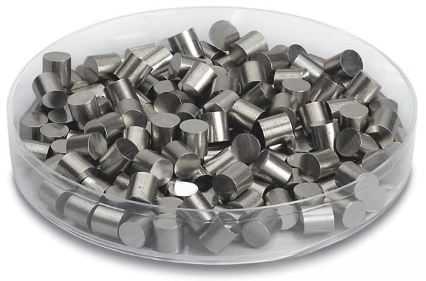
Nickel Chromium Silicon evaporation materials are typically supplied as granules, pellets, tablets, rods, or custom-shaped pieces optimized for resistive heating boats, crucibles, or e-beam sources. The composition ratio (e.g., Ni:Cr:Si = 80:15:5 wt% or customized formulations) can be adjusted to meet specific electrical and structural requirements.
Nickel (Ni) contributes ductility, corrosion resistance, and stable electrical properties.
Chromium (Cr) enhances oxidation resistance and improves film hardness and adhesion to substrates such as glass, ceramics, and semiconductor wafers.
Silicon (Si) refines microstructure, modifies resistivity, and can promote the formation of dense, uniform thin films.
High-purity raw materials (typically 99.9%–99.99%) are vacuum melted or induction alloyed to ensure compositional homogeneity. Tight control of oxygen and trace metallic impurities is essential, as contamination directly influences film resistivity, surface roughness, and long-term reliability in microelectronic devices.
Ni/Cr/Si thin films deposited by evaporation exhibit:
Stable sheet resistance over a wide temperature range
Strong adhesion to oxide, silicon, and metal substrates
Improved oxidation resistance compared to binary Ni/Cr alloys
Good compatibility with multilayer stacks and diffusion barrier systems
These characteristics make the alloy particularly valuable in high-temperature electronics, thin film resistors, and protective conductive coatings.
Applications
Nickel Chromium Silicon evaporation materials are commonly used in:
Thin Film Resistors – Controlled resistivity films for precision electronic components
Semiconductor Metallization – Adhesion or barrier layers in integrated circuits
Display Technologies – Functional conductive layers in flat panel displays
Optical Coatings – Durable underlayers for multilayer optical stacks
Energy Devices – Stable coatings in sensors, heating elements, and power modules
Research & Development – Alloy film studies and material property optimization
The combination of oxidation resistance and electrical stability makes Ni/Cr/Si particularly suitable for environments involving thermal cycling or elevated operating temperatures.
Technical Parameters
| Parameter | Typical Value / Range | Importance |
|---|---|---|
| Purity | 99.9% – 99.99% | Minimizes contamination and improves film consistency |
| Composition Ratio | Custom (e.g., 80:15:5 wt%) | Controls resistivity and film properties |
| Form | Granules / Pellets / Rods | Compatible with various evaporation sources |
| Melting Process | Vacuum Induction Melted | Ensures compositional uniformity |
| Density | ≥ 98% of theoretical | Promotes stable evaporation rate |
| Oxygen Content | ≤ 1000 ppm (typical control) | Reduces film defects and instability |
Comparison with Related Materials
| Material | Key Advantage | Typical Application |
|---|---|---|
| Nickel Chromium Silicon | Improved oxidation resistance & stability | Precision resistive films |
| Nickel Chromium (Ni/Cr) | Mature resistor alloy, stable performance | Thin film resistors |
| Pure Nickel | Good conductivity, ductility | Conductive layers |
| Chromium | Hardness & corrosion resistance | Adhesion layers |
Compared to traditional Ni/Cr alloys, the addition of silicon enhances microstructural stability and can improve film performance under thermal stress, particularly in demanding electronic environments.
FAQ
| Question | Answer |
|---|---|
| Can the product be customized? | Yes, composition ratio, purity level, and physical form can be tailored to your deposition system. |
| Is Ni/Cr/Si suitable for e-beam evaporation? | Yes, it is compatible with both thermal and electron beam evaporation processes. |
| How is film resistivity controlled? | By adjusting the Ni/Cr/Si composition ratio and deposition parameters. |
| What industries use this material most? | Semiconductor, electronics manufacturing, display technology, energy systems, and research laboratories. |
| How is it packaged? | Vacuum-sealed in moisture-barrier packaging with protective cushioning for safe international transport. |
Packaging
Our Nickel Chromium Silicon Evaporation Materials are meticulously tagged and labeled externally to ensure efficient identification and maintain high standards of quality control. We take great care to prevent any potential damage during storage and transportation, ensuring the materials arrive in perfect condition.
Conclusion
Nickel Chromium Silicon Evaporation Materials provide a reliable and versatile solution for high-performance thin film deposition. With tunable composition, stable electrical properties, and excellent oxidation resistance, Ni/Cr/Si alloys support precision applications in electronics, optics, and advanced energy systems.
For detailed specifications and a quotation, please contact us at sales@thinfilmmaterials.com.


Reviews
There are no reviews yet.