 MSDS File
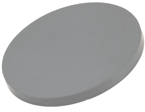
Nickel Ferrite Sputtering Target Description
Nickel ferrite sputtering target from TFM is an alloy sputtering material composed of nickel (Ni) and iron (Fe).
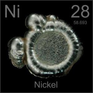
Nickel is a chemical element derived from the German word ‘kupfernickel,’ meaning either devil’s copper or St. Nicholas’s copper. It was first mentioned in 1751 and observed by F. Cronstedt, who also accomplished and announced its isolation. “Ni” is the canonical chemical symbol of nickel. It has an atomic number of 28, situated in Period 4 and Group 10 of the periodic table, belonging to the d-block elements. The relative atomic mass of nickel is 58.6934(2) Daltons, with the number in parentheses indicating the margin of uncertainty.
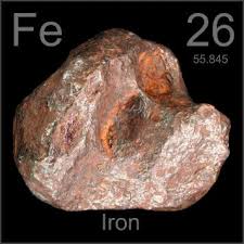
Iron, also known as ferrum, is a chemical element derived from the Anglo-Saxon name “iren” (Latin: “ferrum”). It has been in use since before 5000 BC. The canonical chemical symbol for iron is “Fe.” It holds the atomic number 26 in the periodic table and is located in Period 4 and Group 8, belonging to the d-block. The relative atomic mass of iron is 55.845(2) Daltons, with the number in parentheses indicating the uncertainty.
Related Product: Nickel Sputtering Target, Iron Sputtering Target
Nickel Ferrite Sputtering Target Specification
| Material Type | Nickel Ferrite |
| Symbol | NiFe2O4 |
| Color/Appearance | Gray solid |
| Melting Point | N/A |
| Density | 5.4 g/cm3 |
| Available Sizes | Dia.: 2.0″, 3.0″, 4.0″, 5.0″, 6.0″ Thick: 0.125″, 0.250″ |
We also offer other customized shapes and sizes of the sputtering targets; please Contact Us for more information.
Nickel Ferrite Sputtering Target Packaging
Our nickel ferrite sputter targets are meticulously handled to prevent any damage during storage and transportation. This careful packaging ensures the quality of our products is maintained in their original condition. Each target is clearly tagged and labeled externally to facilitate efficient identification and quality control.
Get Contact
TFM offers Nickel Ferrite Sputtering Targets in various forms, purities, sizes, and prices. We specialize in high-purity thin film deposition materials with optimal density and minimal grain sizes, which are ideal for semiconductor, CVD, and PVD applications in display and optics. Contact Us for current pricing on sputtering targets and other deposition materials that are not listed.


Reviews
There are no reviews yet.