
Nickel Gallium Sputtering Target Description
The Nickel Gallium Sputtering Target is an essential material for thin-film deposition processes. Comprising a high-purity alloy of nickel and gallium, this target offers exceptional thermal stability, ensuring reliable performance even under challenging conditions. Its high electrical conductivity facilitates efficient electron transfer, making it ideal for semiconductor manufacturing and electronic device fabrication. Additionally, the Nickel Gallium Sputtering Target provides excellent adhesion to substrates, resulting in durable and dependable thin films. Its versatility extends to various industries, including optical coatings and magnetic storage devices. Using this target ensures precise and uniform film deposition, contributing to the production of high-performance electronic and optical devices.
Related Product: Aluminum Nickel Sputtering Target, Chromium Nickel Sputtering Target
Nickel Gallium Sputtering Target Specifications
| Compound Formula | Ni/Ga |
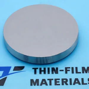
| Appearance | Silver Grey Target |
| Density | 8.53-8.99 g/cm3 |
| Available Sizes | Dia.: 1.0″, 2.0″, 3.0″, 4.0″, 5.0″, 6.0″ Thick: 0.125″, 0.250″ |
Nickel Gallium Sputtering Target Handling Notes
Indium bonding is recommended for the Nickel Gallium Sputtering Target due to certain characteristics that can complicate sputtering, such as brittleness and low thermal conductivity. The target’s low thermal conductivity and susceptibility to thermal shock further highlight the need for appropriate bonding to ensure optimal performance during the sputtering process.
Nickel Gallium Sputtering Target Application
Semiconductor Manufacturing: The Nickel Gallium Sputtering Target is crucial in semiconductor manufacturing. It is used to deposit metal oxide films, metal stacked structures, and conductive layers for the production of transistors, capacitors, and other electronic devices.
Optical Coatings: This target is employed to create optical coatings for mirrors, filters, and lenses. Its excellent optical properties and high reflectivity enhance the efficiency and performance of optical devices.
Magnetic Memory Devices: In magnetic memory devices, the Nickel Gallium Sputtering Target is used to produce magnetic films, such as those for read/write heads in disk drives and magnetic layers in memory storage.
Other Applications: The material is also utilized for preparing conductive coatings, anti-corrosion coatings, and various functional coatings. It finds applications across electronics, optics, materials science, and other fields.
Nickel Gallium Sputtering Target Packaging
We take great care in handling our Nickel Gallium Sputtering Target during storage and transportation to ensure it maintains its original quality and condition.
Get Contact
TFM provides Nickel Gallium Sputtering Targets in a range of forms, purities, and sizes. We specialize in producing high-purity physical vapor deposition (PVD) materials with maximum density and minimal average grain sizes, making them ideal for use in semiconductor applications, chemical vapor deposition (CVD), and PVD processes for display and optical technologies.


Reviews
There are no reviews yet.