
Introduction
The Niobium Diboride Sputtering Target (NbB₂) is a high-performance ceramic target used in thin film deposition processes for applications requiring exceptional hardness, thermal stability, and electrical conductivity. Niobium diboride belongs to the family of ultra-high-temperature ceramic (UHTC) materials, known for their ability to maintain structural and chemical stability under extreme conditions.
NbB₂ thin films deposited via magnetron sputtering or other physical vapor deposition (PVD) techniques are widely studied for wear-resistant coatings, conductive ceramic films, diffusion barriers, and high-temperature protective layers. Due to its unique combination of metallic conductivity and ceramic hardness, NbB₂ is increasingly used in advanced electronics, aerospace coatings, and research on next-generation functional materials.
Detailed Description
Niobium Diboride sputtering targets are typically produced using high-purity niobium and boron powders through advanced ceramic processing methods such as hot pressing, spark plasma sintering (SPS), or hot isostatic pressing (HIP). These manufacturing techniques help achieve high density, uniform microstructure, and stable stoichiometry, which are essential for reliable sputtering performance.
NbB₂ is characterized by an extremely high melting point (above 3000 °C), excellent hardness, and good electrical conductivity compared with many traditional ceramic materials. This combination makes it particularly valuable for thin films that must operate in harsh environments or at elevated temperatures.
When used as a sputtering target, NbB₂ enables the deposition of thin films that exhibit strong adhesion, high wear resistance, and good thermal conductivity. These properties are important in protective coatings, microelectronic barrier layers, and specialized functional films.
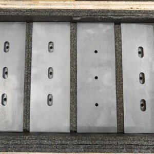
High-density NbB₂ targets help maintain stable sputtering rates and reduce particle generation during deposition. For high-power sputtering systems, targets can also be supplied with copper backing plates using indium or diffusion bonding, which improves heat dissipation and mechanical stability during operation.
Applications
Niobium Diboride sputtering targets are used across several advanced technology sectors:
Wear-resistant coatings for cutting tools and industrial components
Diffusion barrier layers in semiconductor devices
High-temperature protective coatings in aerospace and extreme environments
Conductive ceramic thin films used in microelectronics
Advanced coating research involving boride-based materials
Vacuum and plasma system components requiring durable surface coatings
Technical Parameters
| Parameter | Typical Value / Range | Importance |
|---|---|---|
| Purity | 99.5% – 99.9% | Higher purity ensures stable thin film properties |
| Chemical Formula | NbB₂ | Determines boride structure and electrical conductivity |
| Diameter | 25 – 300 mm (custom) | Compatible with various sputtering systems |
| Thickness | 3 – 6 mm | Influences sputtering efficiency and target life |
| Density | ≥ 95% theoretical density | Ensures uniform deposition and stable sputtering |
| Bonding | Copper backing plate / Indium bonded | Improves heat transfer and target stability |
Comparison with Related Materials
| Material | Key Advantage | Typical Application |
|---|---|---|
| Niobium Diboride (NbB₂) | High hardness with electrical conductivity | Protective and conductive ceramic coatings |
| Titanium Diboride (TiB₂) | Extremely high hardness and wear resistance | Cutting tools and protective coatings |
| Tungsten Boride (WB/WB₂) | High thermal stability and hardness | High-temperature protective films |
FAQ
| Question | Answer |
|---|---|
| What sputtering methods are compatible with NbB₂ targets? | NbB₂ sputtering targets are commonly used in RF magnetron sputtering and other PVD deposition systems suitable for ceramic materials. |
| Can the target size be customized? | Yes. Diameter, thickness, and bonding configurations can be tailored to specific sputtering systems. |
| Are bonded sputtering targets available? | Yes. NbB₂ targets can be bonded to copper backing plates using indium or diffusion bonding to improve heat dissipation. |
| What purity levels are typically available? | Standard purity levels range from 99.5% to 99.9%. |
| What substrates can NbB₂ thin films be deposited on? | NbB₂ films can be deposited on metals, ceramics, silicon wafers, and glass substrates. |
Packaging
Our Niobium Diboride Sputtering Target (NbB₂) products are meticulously tagged and labeled externally to ensure efficient identification and maintain strict quality control standards. Each target is packaged using vacuum-sealed bags, protective foam materials, and export-grade cartons or wooden crates to prevent contamination, oxidation, and mechanical damage during storage and transportation.
Conclusion
The Niobium Diboride Sputtering Target (NbB₂) provides an effective material solution for producing durable, high-performance thin films used in extreme environments and advanced electronic applications. Its combination of ceramic hardness, electrical conductivity, and thermal stability makes it particularly suitable for wear-resistant coatings, diffusion barriers, and high-temperature protective layers.
With customizable sizes, high-density manufacturing, and reliable sputtering performance, NbB₂ sputtering targets support both industrial coating processes and cutting-edge materials research.
For detailed specifications and a quotation, please contact us at sales@thinfilmmaterials.com.


Reviews
There are no reviews yet.