Generic selectors
Exact matches only
Search in title
Search in content
Post Type Selectors

VD0851 Niobium Diselenide Evaporation Materials, NbSe2

Catalog No.VD0851
MaterialNiobium Selenide (NbSe2)
Purity99.9% ~ 99.999%
ShapePowder/ Granule/ Custom-made

TFM stands out as a premier producer and distributor of high-purity niobium diselenide evaporation materials. In addition to niobium diselenide, we provide a diverse range of evaporation materials tailored to meet various needs. Our products are available in both powder and granule forms, with customized options offered upon request to ensure they meet your specific requirements.

Niobium Diselenide Evaporation Materials Overview

Niobium diselenide (NbSe₂) evaporation materials, offered by TFM, are high-quality selenide ceramic materials crucial for various deposition processes. With a chemical formula of NbSe₂, these materials are essential for creating high-purity deposited films. TFM is committed to producing niobium diselenide with exceptional purity levels, up to 99.9995%, ensuring reliable and consistent results.

Niobium Diselenide Evaporation Materials Specification
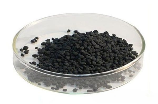
Material TypeNiobium Diselenide
SymbolNbSe2
Appearance/ColorGray solid
Melting Point>1300 °C
Density6.3 g/cm3
Purity99.9% ~ 99.999%
ShapePowder/ Granule/ Custom-made

Applications

Niobium diselenide evaporation materials are versatile and used in a range of deposition techniques, including:

  • Semiconductor Deposition
  • Chemical Vapor Deposition (CVD)
  • Physical Vapor Deposition (PVD)

These materials are particularly valuable for optical applications such as:

  • Wear Protection
  • Decorative Coatings
  • Display Technologies

Packaging and Handling

TFM ensures that niobium diselenide evaporation materials are packaged with clear labeling for easy identification and quality control. The packaging is designed to prevent damage during storage and transportation, maintaining the integrity of the product.

Contact Us

As a premier provider of high-purity niobium diselenide evaporation materials, TFM offers a range of forms, including tablets, granules, rods, and wires. Custom shapes and quantities are available upon request. We also supply evaporation sources, boats, filaments, crucibles, heaters, and e-beam crucible liners. For current pricing and additional information, please reach out with your inquiry.

Reviews

There are no reviews yet.

Be the first to review “VD0851 Niobium Diselenide Evaporation Materials, NbSe2”

Your email address will not be published. Required fields are marked *

FAQ

  • They are high‐purity substances (e.g. metals, alloys, or compounds) used in thermal or electron‐beam evaporation processes to form thin films on substrates.

  • Typically, they’re processed into a form (often ingots, pellets, or wires) that can be efficiently vaporized. Preparation emphasizes high purity and controlled composition to ensure film quality.

  • Thermal evaporation and electron-beam (e-beam) evaporation are the two main techniques, where material is heated (or bombarded with electrons) until it vaporizes and then condenses on the substrate.

  • Thermal evaporation heats the material directly (often using a resistive heater), while e-beam evaporation uses a focused electron beam to locally heat and vaporize the source material—each method offering different control and energy efficiency.

  • Key parameters include source temperature, vacuum level, deposition rate, substrate temperature, and the distance between the source and the substrate. These factors influence film uniformity, adhesion, and microstructure.

  • Evaporation generally produces high-purity films with excellent control over thickness, and it is especially suitable for materials with relatively low melting points or high vapor pressures.

  • Challenges include issues with step coverage (due to line-of-sight deposition), shadowing effects on complex topographies, and possible re-evaporation of material from the substrate if temperature isn’t properly controlled.

  • Common evaporation materials include noble metals (e.g., gold, silver), semiconductors (e.g., silicon, germanium), metal oxides, and organic compounds—each chosen for its specific optical, electrical, or mechanical properties.

  • Selection depends on desired film properties (conductivity, optical transparency, adhesion), compatibility with the evaporation process, and the final device application (semiconductor, optical coating, etc.).

  • Optimizing substrate temperature, deposition rate, and chamber vacuum are critical for ensuring that the film adheres well and forms the intended microstructure without defects.

  • Troubleshooting may involve checking the source material’s purity, ensuring stable source temperature, verifying the vacuum level, adjusting the substrate’s position or temperature, and monitoring deposition rate fluctuations.

While evaporation tends to yield very high purity films with excellent thickness control, it is limited by its line-of-sight nature. In contrast, sputtering can deposit films more uniformly on complex surfaces and is more versatile for a broader range of materials.


Shopping Cart
Scroll to Top