Generic selectors
Exact matches only
Search in title
Search in content
Post Type Selectors

VD0719 Niobium(V) Oxide Evaporation Materials, Nb2O5

Material Type: Niobium (V) Oxide
Symbol: Nb2O5
Color/Appearance: White Solid
Purity: 99.9% ~ 99.95%
Shape: Powder/ Granule/ Custom-made

TFM is a top manufacturer and supplier of high-purity niobium(V) oxide evaporation materials, as well as a broad selection of other evaporation materials. We provide these materials in powder and granule forms, with the option to customize shapes according to your specific requirements.

Niobium(V) Oxide Evaporation Materials Overview

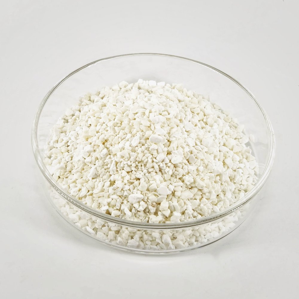
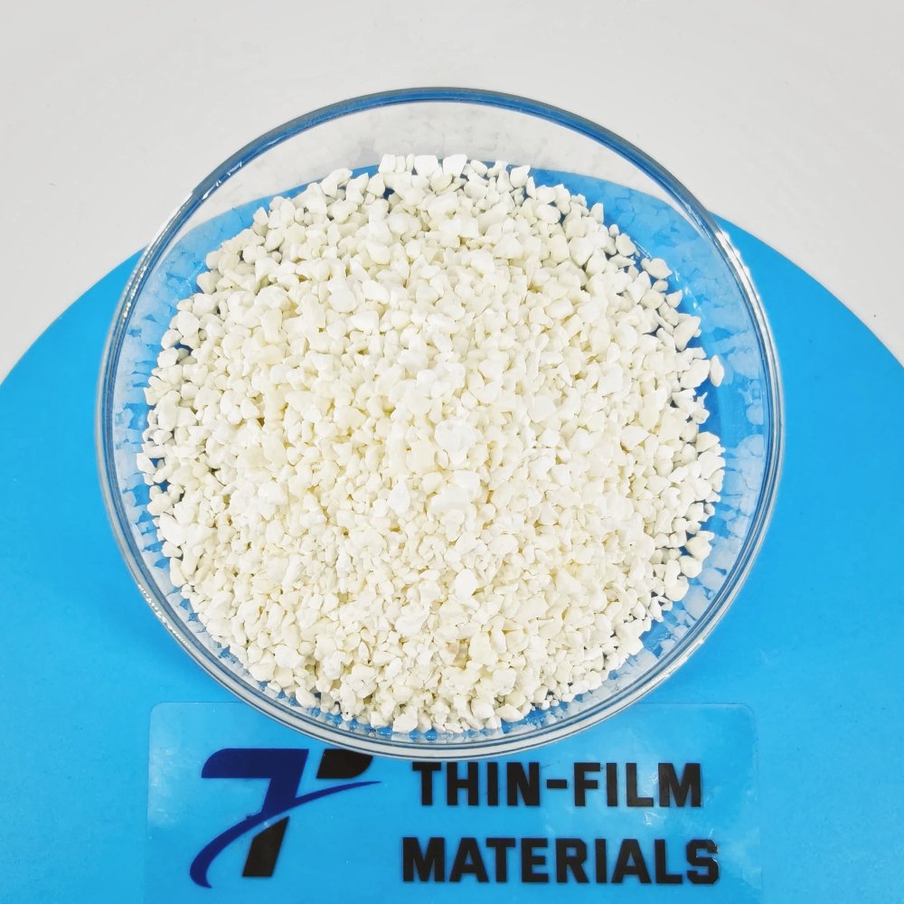
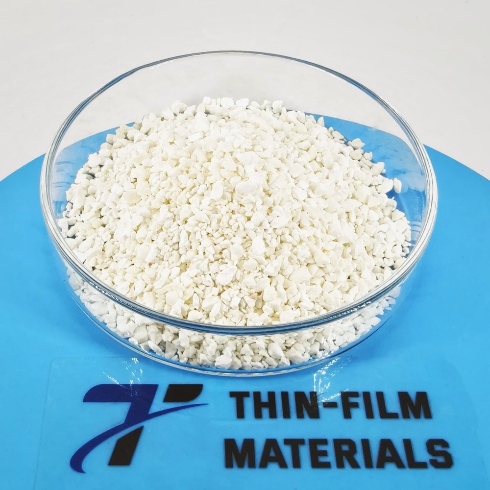
Niobium(V) oxide (Nb₂O₅) is a high-purity oxide evaporation material essential for producing high-quality thin films in various deposition processes. With purity levels reaching up to 99.9995%, Nb₂O₅ is crucial for ensuring the reliability and performance of the deposited films. TFM specializes in manufacturing this material under strict quality control standards, guaranteeing consistency and dependability in every batch.

Niobium(V) Oxide Evaporation Materials Specification

Material TypeNiobium(V) oxide
SymbolNb2O5
Color/AppearanceWhite Solid
Melting Point1,485°C
Theoretical Density 4.60 g/cm3
Purity99.9% ~ 99.95%
ShapePowder/ Pellets/ Granule/ Custom-made

Applications of Niobium(V) Oxide Evaporation Materials

Niobium(V) oxide is widely used in several applications, including:

  • Deposition Processes: Integral to semiconductor deposition, chemical vapor deposition (CVD), and physical vapor deposition (PVD).
  • Optical Coatings: Used for wear protection, decorative coatings, and in display technologies.

Packaging and Quality Assurance

Our niobium(V) oxide evaporation materials are carefully tagged and labeled to ensure easy identification and maintain high quality. The packaging is designed to protect the materials from damage during storage and transportation, ensuring they arrive in perfect condition.

Contact Us

TFM is a leading supplier of high-purity niobium(V) oxide evaporation materials, offering a variety of shapes including tablets, granules, rods, and wires. Customized forms and quantities are available upon request. We also provide evaporation sources, boats, filaments, crucibles, heaters, and e-beam crucible liners. For inquiries about pricing or materials not listed, please contact us.

Reviews

There are no reviews yet.

Be the first to review “VD0719 Niobium(V) Oxide Evaporation Materials, Nb2O5”

Your email address will not be published. Required fields are marked *

FAQ

  • They are high‐purity substances (e.g. metals, alloys, or compounds) used in thermal or electron‐beam evaporation processes to form thin films on substrates.

  • Typically, they’re processed into a form (often ingots, pellets, or wires) that can be efficiently vaporized. Preparation emphasizes high purity and controlled composition to ensure film quality.

  • Thermal evaporation and electron-beam (e-beam) evaporation are the two main techniques, where material is heated (or bombarded with electrons) until it vaporizes and then condenses on the substrate.

  • Thermal evaporation heats the material directly (often using a resistive heater), while e-beam evaporation uses a focused electron beam to locally heat and vaporize the source material—each method offering different control and energy efficiency.

  • Key parameters include source temperature, vacuum level, deposition rate, substrate temperature, and the distance between the source and the substrate. These factors influence film uniformity, adhesion, and microstructure.

  • Evaporation generally produces high-purity films with excellent control over thickness, and it is especially suitable for materials with relatively low melting points or high vapor pressures.

  • Challenges include issues with step coverage (due to line-of-sight deposition), shadowing effects on complex topographies, and possible re-evaporation of material from the substrate if temperature isn’t properly controlled.

  • Common evaporation materials include noble metals (e.g., gold, silver), semiconductors (e.g., silicon, germanium), metal oxides, and organic compounds—each chosen for its specific optical, electrical, or mechanical properties.

  • Selection depends on desired film properties (conductivity, optical transparency, adhesion), compatibility with the evaporation process, and the final device application (semiconductor, optical coating, etc.).

  • Optimizing substrate temperature, deposition rate, and chamber vacuum are critical for ensuring that the film adheres well and forms the intended microstructure without defects.

  • Troubleshooting may involve checking the source material’s purity, ensuring stable source temperature, verifying the vacuum level, adjusting the substrate’s position or temperature, and monitoring deposition rate fluctuations.

While evaporation tends to yield very high purity films with excellent thickness control, it is limited by its line-of-sight nature. In contrast, sputtering can deposit films more uniformly on complex surfaces and is more versatile for a broader range of materials.


Shopping Cart
Scroll to Top