 MSDS File
Introduction
Niobium Telluride (NbTe₂) Evaporation Materials are specialized compounds used in thin film deposition processes for advanced electronic, optical, and quantum materials research. As a transition metal dichalcogenide (TMD), NbTe₂ exhibits unique layered crystal structures and intriguing electronic properties, including metallic conductivity, charge density wave behavior, and potential applications in emerging nanoelectronic devices.
In Physical Vapor Deposition (PVD) processes such as thermal evaporation and electron beam evaporation, NbTe₂ evaporation materials enable the fabrication of high-quality thin films with controlled stoichiometry. These materials are widely used in condensed matter physics research, two-dimensional materials studies, and advanced semiconductor device development.
Detailed Description
Niobium Telluride (NbTe₂) belongs to the family of transition metal dichalcogenides, a group of layered materials characterized by strong in-plane covalent bonding and weak interlayer van der Waals interactions. This layered structure enables NbTe₂ to exhibit anisotropic electrical and optical properties, making it a promising material for next-generation electronic and optoelectronic applications.
In its crystalline form, NbTe₂ consists of niobium atoms sandwiched between two layers of tellurium atoms, forming a stable Te–Nb–Te structure. The material exhibits metallic conductivity and complex electronic phenomena such as charge density waves, which are of significant interest in condensed matter physics and quantum materials research.
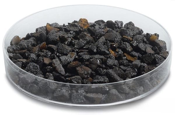
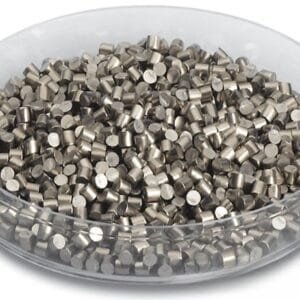
When used as an evaporation material, NbTe₂ is typically supplied in the form of granules, pellets, or pieces suitable for loading into evaporation sources such as crucibles or boats. High-purity NbTe₂ ensures that the deposited thin films maintain accurate stoichiometry and minimal contamination, which is crucial for preserving the electronic properties of the material.
During the evaporation process, the NbTe₂ source material vaporizes under high vacuum conditions and condenses onto substrates to form thin films. Careful control of deposition parameters—such as substrate temperature, evaporation rate, and vacuum level—allows researchers to achieve uniform films with controlled thickness and crystal structure.
NbTe₂ thin films are particularly valuable in the exploration of two-dimensional materials and layered heterostructures. Their unique electronic characteristics make them suitable for studying electron correlation effects, topological phases, and nanoscale device behavior.
Applications
Niobium Telluride evaporation materials are primarily used in advanced research and high-tech thin film fabrication. Common applications include:
Two-dimensional materials research involving transition metal dichalcogenides
Nanoelectronic and quantum devices
Charge density wave (CDW) materials studies
Layered heterostructures and van der Waals devices
Thin film electronic and optoelectronic components
Materials science and condensed matter physics research
These applications make NbTe₂ an important compound in emerging electronic and quantum technologies.
Technical Parameters
| Parameter | Typical Value / Range | Importance |
|---|---|---|
| Purity | 99.9% – 99.999% | Higher purity improves film quality and electronic performance |
| Chemical Formula | NbTe₂ | Ensures correct compound stoichiometry |
| Form | Granules / Pellets / Pieces | Suitable for evaporation sources |
| Particle Size | 1 – 6 mm typical | Influences evaporation stability |
| Density | ~7.3 g/cm³ | Affects evaporation behavior |
| Deposition Method | Thermal / E-Beam Evaporation | Compatible with common PVD systems |
Comparison with Related Materials
| Material | Key Advantage | Typical Application |
|---|---|---|
| Niobium Telluride (NbTe₂) | Metallic conductivity and layered structure | Quantum materials and nanoelectronics |
| Molybdenum Disulfide (MoS₂) | Semiconductor behavior | 2D electronics and transistors |
| Tungsten Diselenide (WSe₂) | Strong optical properties | Optoelectronic devices |
| Niobium Diselenide (NbSe₂) | Superconductivity and charge density waves | Quantum electronic devices |
FAQ
| Question | Answer |
|---|---|
| Can NbTe₂ evaporation materials be customized? | Yes, the purity level, particle size, and packaging can be customized according to deposition system requirements. |
| What deposition techniques are compatible with NbTe₂ evaporation materials? | NbTe₂ is typically used in thermal evaporation or electron beam evaporation systems. |
| Why is NbTe₂ important for research applications? | NbTe₂ exhibits unique electronic properties such as metallic conductivity and charge density wave behavior, making it valuable for quantum materials research. |
| What substrates are commonly used for NbTe₂ thin films? | Common substrates include silicon wafers, sapphire, glass, and layered materials used in heterostructure research. |
| How should NbTe₂ evaporation materials be stored? | They should be stored in sealed containers under dry conditions to prevent contamination or oxidation. |
Packaging
Our Niobium Telluride Evaporation Materials are meticulously tagged and labeled externally to ensure efficient identification and maintain high standards of quality control. We take great care to prevent any potential damage during storage and transportation, ensuring the targets arrive in perfect condition.
Conclusion
Niobium Telluride (NbTe₂) evaporation materials provide a reliable source for producing layered transition metal dichalcogenide thin films with unique electronic and structural properties. Their metallic conductivity and layered crystal structure make them valuable for advanced research in quantum materials, nanoelectronics, and thin film heterostructures.
With customizable purity levels, particle sizes, and packaging options, NbTe₂ evaporation materials are suitable for both experimental research and advanced thin film deposition systems.
For detailed specifications and a quotation, please contact us at sales@thinfilmmaterials.com.


Reviews
There are no reviews yet.