
 MSDS File
Introduction
P-type Silicon Evaporation Materials (Si) are essential sources for depositing doped silicon thin films in semiconductor, photovoltaic, and microelectronic applications. By introducing controlled acceptor dopants—typically boron—into high-purity silicon, P-type Si enables the formation of hole-conducting layers required in PN junctions, thin film transistors, and advanced device structures.
In physical vapor deposition (PVD) systems such as thermal evaporation and electron beam evaporation, the electrical characteristics of the deposited film strongly depend on dopant concentration, purity, and evaporation stability. Carefully prepared P-type Silicon evaporation materials ensure reproducible conductivity and consistent film quality across research and industrial production lines.
Detailed Description
P-type Silicon Evaporation Materials are manufactured from electronic-grade silicon that has been precisely doped with acceptor elements, most commonly boron (B). The dopant concentration is tightly controlled to achieve target resistivity ranges suitable for specific device architectures.
Key characteristics include:
Controlled Dopant Level – Ensures predictable resistivity and carrier concentration in deposited films.
High Chemical Purity (typically 4N–6N base Si) – Minimizes metallic and oxygen contamination that could affect semiconductor performance.
Stable Evaporation Behavior – Uniform melting and vaporization reduce spitting and compositional fluctuation.
Custom Resistivity Range – Available from low-resistivity (heavily doped) to higher-resistivity grades depending on application.
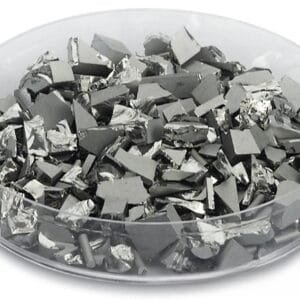
Material forms include pieces, chunks, granules, or pellets compatible with tungsten boats, molybdenum crucibles, or graphite liners. For high-temperature e-beam evaporation, gradual power ramping is recommended to minimize thermal stress and avoid cracking.
During evaporation, dopant distribution in the vapor phase must remain stable to ensure consistent electrical properties in the deposited thin film. Therefore, homogeneity of the starting material is critical.
Applications
P-type Silicon Evaporation Materials are widely used in:
Semiconductor Device Fabrication
Deposition of doped silicon layers for diodes, transistors, and integrated circuits.Photovoltaic Thin Films
Formation of P-type layers in thin film solar cells and heterojunction devices.MEMS & Microelectronics
Functional silicon coatings requiring defined conductivity.Research & Development
Experimental doping studies and thin film semiconductor engineering.Sensor Technologies
Fabrication of silicon-based sensing elements with tailored electrical response.
Technical Parameters
| Parameter | Typical Value / Range | Importance |
|---|---|---|
| Base Silicon Purity | 99.99% – 99.9999% (4N–6N) | Reduces contamination in semiconductor films |
| Dopant Type | Boron (B) typical | Creates P-type conductivity |
| Resistivity | 0.001 – 10 Ω·cm (customizable) | Defines carrier concentration |
| Form | Pieces / Granules / Pellets | Compatible with evaporation sources |
| Melting Point | 1414°C | Suitable for thermal and e-beam evaporation |
| Packaging | Vacuum-sealed or inert atmosphere | Prevents oxidation and contamination |
Comparison with Related Materials
| Material | Key Advantage | Typical Application |
|---|---|---|
| P-type Silicon (Si) | Controlled hole conductivity | PN junction layers |
| N-type Silicon (Si) | Electron-conducting properties | Complementary semiconductor layers |
| Intrinsic Silicon | Minimal dopant influence | Baseline or insulating studies |
| Silicon Monoxide (SiO) | Oxide film formation capability | Optical and dielectric coatings |
Compared with intrinsic or N-type silicon, P-type silicon is specifically engineered to introduce acceptor states, enabling controlled electrical functionality in deposited films.
FAQ
| Question | Answer |
|---|---|
| Can the resistivity be customized? | Yes, dopant concentration and resistivity can be tailored to specific device requirements. |
| Is P-type Si suitable for thermal evaporation? | Yes, it is compatible with both thermal and electron beam evaporation systems. |
| How is dopant uniformity ensured? | The material is prepared from homogenized, pre-doped silicon to maintain consistent composition. |
| What forms are available? | Pieces, granules, and pellets are available to match different source designs. |
| Which industries use P-type silicon most? | Semiconductor manufacturing, photovoltaics, MEMS, sensors, and R&D institutions. |
Packaging
Our P-type Silicon Evaporation Materials are meticulously tagged and labeled externally to ensure efficient identification and maintain high standards of quality control. We take great care to prevent any potential damage during storage and transportation, ensuring the materials arrive in perfect condition.
Conclusion
P-type Silicon Evaporation Materials (Si) provide a dependable and customizable solution for depositing doped silicon thin films with defined electrical properties. With controlled purity, tailored resistivity, and flexible supply formats, they support both precision semiconductor research and large-scale device manufacturing.
For detailed specifications and a quotation, please contact us at sales@thinfilmmaterials.com.


Reviews
There are no reviews yet.