
 MSDS File
| Material Type | PbxSn1-xAs |
| Symbol | PbxSn1-xAs |
| Melting Point (°C) | |
| Theoretical Density (g/cc) |
| Z Ratio | |
| E-Beam | |
| E-Beam Crucible Liner Material | |
| Temp. (°C) for Given Vap. Press. (Torr) | |
| Comments |
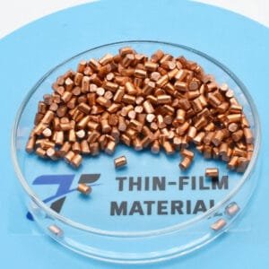
PbxSn1-xAs Evaporation Material
TFM offers high-purity PbxSn1-xAs Evaporation Material, engineered for thin-film deposition in advanced semiconductor, optoelectronic, and infrared detection applications. This material, composed of lead (Pb), tin (Sn), and arsenic (As), exhibits tunable electronic and optical properties, making it highly suitable for next-generation infrared (IR) sensors, thermoelectric devices, and optoelectronic components.
Optimized for thermal evaporation and electron beam (E-beam) evaporation, PbxSn1-xAs Evaporation Material ensures precise stoichiometry control, high film uniformity, and excellent adhesion to various substrates.
Key Features and Advantages
Adjustable Bandgap & Electronic Properties: The Pb-Sn-As composition enables bandgap engineering, enhancing its performance for infrared detection and optoelectronic applications.
High Purity & Low Defect Density: Ensures uniform thin-film deposition with minimal impurities, improving device efficiency and reliability.
Superior Infrared Absorption: Ideal for thermal imaging, IR sensors, and night-vision applications.
Stable Chemical & Thermal Behavior: Maintains structural integrity under high-temperature processing conditions, ensuring long-term performance.
Customizable Stoichiometry (PbxSn1-xAs): Available in various Pb/Sn ratios, allowing precise tuning of electrical and optical properties for specific applications.
Applications
Infrared & Thermal Imaging Sensors: Used in IR detectors, thermal cameras, and night-vision systems.
Optoelectronic & Photodetector Devices: Plays a key role in photoelectric conversion and infrared communication.
Semiconductor & Energy Harvesting Devices: Supports thermoelectric applications for waste heat recovery and energy efficiency.
Thin-Film Transistors (TFTs): Provides high carrier mobility for next-generation electronic circuits.
Industry Impact and Customization
TFM’s PbxSn1-xAs Evaporation Material enables innovations in infrared detection, optoelectronics, and semiconductor research, offering custom material compositions to meet specific industry requirements. Our precision manufacturing ensures high film quality, controlled stoichiometry, and superior performance, making it a reliable choice for cutting-edge thin-film coatings.
With its exceptional electrical, optical, and thermal properties, TFM’s PbxSn1-xAs Evaporation Material is an essential material for high-performance infrared sensors, optoelectronic devices, and semiconductor applications, delivering optimized efficiency and long-term stability.


Reviews
There are no reviews yet.