Introduction
Planar Tungsten (W) Sputtering Targets are critical deposition materials widely used in semiconductor manufacturing, microelectronics, and advanced thin film applications. Tungsten’s exceptional melting point, low vapor pressure, and excellent electrical conductivity make it a preferred material for forming dense, stable films in demanding sputtering environments.
Detailed Description
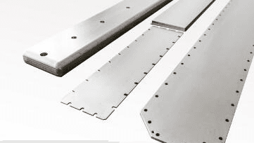
Planar tungsten sputtering targets are manufactured from high-purity tungsten using carefully controlled powder metallurgy and densification processes. These steps ensure uniform grain structure, high density, and consistent composition across the entire target surface—key factors for achieving stable sputtering rates and uniform film thickness.
Due to tungsten’s hardness and high melting point, precision machining is essential. Each planar target is finished to tight flatness and thickness tolerances to ensure proper bonding (when required) and efficient heat dissipation during sputtering. Targets may be supplied unbonded for smaller sizes or bonded to copper backing plates for improved thermal conductivity and mechanical stability in high-power magnetron sputtering systems.
Tungsten targets exhibit excellent resistance to deformation, low particulate generation, and long service life, supporting reliable deposition in both R&D and volume production settings.
Applications
Semiconductor interconnects and barrier layers
Thin film resistors and conductive coatings
Integrated circuits and MEMS devices
Display panels and flat panel electronics
Research-scale PVD and materials science studies
Technical Parameters
| Parameter | Typical Value / Range | Importance |
|---|---|---|
| Material | Tungsten (W) | High melting point, stable sputtering |
| Purity | 99.95% – 99.999% | Impurity control affects film performance |
| Target Type | Planar (rectangular or circular) | Compatible with planar magnetrons |
| Diameter / Size | Custom sizes available | Matches sputtering cathodes |
| Thickness | 3 – 10 mm (typical) | Influences target lifetime |
| Backing Plate | Copper (optional) | Enhances heat transfer |
Comparison with Related Materials
| Material | Key Advantage | Typical Application |
|---|---|---|
| Tungsten (W) | High thermal stability | Semiconductor metallization |
| Molybdenum (Mo) | Lower density, easier machining | Display & electronics |
| Tantalum (Ta) | Excellent barrier properties | Advanced IC fabrication |
FAQ
| Question | Answer |
|---|---|
| Can planar tungsten targets be customized? | Yes, size, thickness, purity, and bonding can be tailored. |
| Are bonded targets available? | Yes, copper-backed tungsten targets are available for high-power use. |
| Is tungsten suitable for DC sputtering? | Yes, tungsten is commonly used with DC magnetron sputtering. |
| How is target flatness controlled? | Precision grinding and inspection ensure tight tolerances. |
| Is a Certificate of Analysis provided? | Yes, CoA is available upon request. |
Packaging
Our Planar Tungsten (W) Sputtering Targets are carefully cleaned, labeled, and vacuum-sealed to prevent contamination. Each target is protected with shock-absorbing materials and packed in export-grade cartons or wooden crates to ensure safe transportation.
Conclusion
Planar Tungsten (W) Sputtering Targets offer excellent durability, stable sputtering behavior, and high purity for advanced thin film deposition. With flexible customization options and strict quality control, they are a reliable choice for semiconductor manufacturing, electronics, and research-driven PVD applications.
For detailed specifications and a quotation, please contact us at sales@thinfilmmaterials.com.


Reviews
There are no reviews yet.