
 MSDS File
Platinum Evaporation Materials
Introduction
Platinum Evaporation Materials are premium-grade sources designed for thin film deposition in advanced research and industrial applications. Known for its exceptional chemical stability, high melting point, and superior catalytic activity, platinum is indispensable in microelectronics, optics, catalysis, and energy systems. Thin films derived from platinum evaporation materials exhibit outstanding durability, corrosion resistance, and electrical conductivity, making them a critical choice for high-performance coatings.
Detailed Description
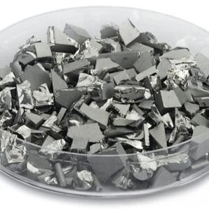
Platinum evaporation materials are typically supplied in pellets, pieces, slugs, granules, or rods, all manufactured from high-purity platinum (99.95%–99.999%). These materials are compatible with both thermal and electron beam (e-beam) evaporation systems.
Key features include:
High Purity (99.95%–99.999%): Ensures defect-free and contamination-free thin films.
Excellent Thermal Stability: With a melting point of 1,768 °C, platinum withstands demanding evaporation conditions.
Outstanding Corrosion Resistance: Inert to most acids and chemicals, ensuring film longevity.
Superior Electrical Conductivity: Provides reliable metallization layers for microelectronics.
Catalytic Properties: Useful for thin films in fuel cells, hydrogen sensors, and catalytic converters.
Applications
Platinum evaporation materials are applied in a wide range of industries:
Microelectronics & Semiconductors: Metallization layers, diffusion barriers, and contacts.
Optical Coatings: Reflective and protective coatings for high-precision optics.
Catalysis: Thin films for fuel cells, hydrogen generation, and chemical processing.
Energy Devices: Electrodes for solid oxide fuel cells, electrolyzers, and batteries.
Medical & Research: Coatings for biomedical devices, sensors, and high-temperature experiments.
Technical Parameters
| Parameter | Typical Value / Range | Importance |
|---|---|---|
| Purity | 99.95% – 99.999% | High purity ensures reliable thin film performance |
| Forms Available | Pellets, pieces, rods, slugs, granules | Compatible with different evaporation sources |
| Melting Point | 1,768 °C | High melting point allows stable deposition |
| Density | 21.45 g/cm³ | Contributes to film density and durability |
| Evaporation Method | Thermal / e-beam | Flexible for different deposition systems |
Comparison with Related Materials
| Material | Key Advantage | Typical Application |
|---|---|---|
| Platinum (Pt) | Excellent chemical stability & catalytic activity | Semiconductors, fuel cells, catalysis |
| Gold (Au) | Highest electrical conductivity | Microelectronics, decoration |
| Palladium (Pd) | Hydrogen absorption & catalytic use | Sensors, membranes, hydrogen purification |
FAQ
| Question | Answer |
|---|---|
| What forms are available? | Platinum is supplied as pellets, slugs, granules, rods, and custom pieces. |
| Can it be customized? | Yes, purity, size, and form can be tailored for specific evaporation systems. |
| How is it packaged? | Vacuum-sealed or argon-filled containers with protective foam and export-safe cartons. |
| What is the delivery time? | Standard lead time is 2–3 weeks, depending on customization. |
| Which industries use it most? | Semiconductors, optics, catalysis, medical devices, and energy. |
Packaging
Platinum evaporation materials are vacuum-sealed or argon-protected to prevent contamination. Each batch is carefully labeled with purity, lot number, and form for full traceability. Export packaging includes protective cartons or wooden crates to ensure safe transport.
Conclusion
The Platinum Evaporation Materials provide unmatched reliability for thin film deposition, offering high purity, excellent stability, and superior catalytic performance. Whether in semiconductors, energy devices, or advanced optics, platinum remains one of the most valuable and versatile evaporation sources available.
For detailed specifications and a quotation, please contact us at sales@thinfilmmaterials.com.


Reviews
There are no reviews yet.