Generic selectors
Exact matches only
Search in title
Search in content
Post Type Selectors

ST0042 Selenium Sputtering Target, Se

Chemical Formula: Se
Catalog Number: ST0042
CAS Number: 7782-49-2
Purity: >99.99%, 99.999%
Shape: Discs, Plates, Column Targets, Step Targets, Custom-made

Selenium  sputtering target  come in various forms, purities, sizes, and prices. Thin Film Materials (TFM) manufactures and supplies top-quality sputtering targets at competitive prices.

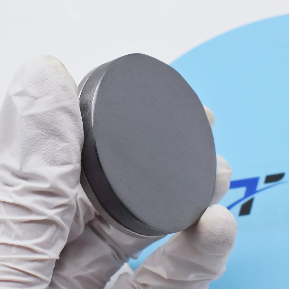
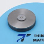
Selenium Sputtering Target Description

Selenium

The selenium sputtering target is a gray material composed of high-purity selenium metal. Selenium, symbolized as “Se,” is a chemical element named after the Greek word for the Moon, “Selene.” It was first mentioned in 1817 and discovered by J. Berzelius and G. Gahn, who later succeeded in isolating it. Selenium has an atomic number of 34 and is located in Period 4, Group 16 of the periodic table, within the p-block. Its relative atomic mass is 78.96 Daltons, with the number in brackets indicating the measurement uncertainty.

Selenium Sputtering Target Specification
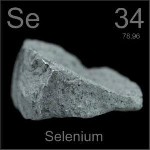
Material TypeSelenium
SymbolSe
Color/AppearanceGray, Metallic Luster, Non-Metallic
Melting Point217 °C
Density4.79 g/cm3
Thermal Conductivity0.00519 W·m-1·K-1 (25°C)
Thermal Expansion37 µm/(m·K) (25°C)
Available SizesDia.: 1.0″, 2.0″, 3.0″, 4.0″, 5.0″, 6.0″
Thick: 0.125″, 0.250″

We also offer other customized shapes and sizes of the sputtering targets; please Contact Us for more information.

Selenium Sputtering Target Bonding Service

Specialized bonding services for Selenium Sputtering Targets, including indium and elastomeric bonding techniques, enhance performance and durability. Thin Film Materials (TFM) ensures high-quality solutions that meet industry standards and customer needs.

We also offer custom machining of backing plates, which is essential for sputtering target assembly. This comprehensive approach improves target design flexibility and performance in thin film deposition. Our channels provide detailed information about bonding materials, methods, and services, helping clients make informed decisions.

Applications of Selenium Sputtering Target

The selenium sputtering target is utilized in various applications, including:

  • Thin film deposition
  • Decoration
  • Semiconductor manufacturing
  • Displays
  • LED and photovoltaic devices
  • Functional coatings
  • Optical information storage
  • Glass coating for automotive and architectural glass
  • Optical communications

Other Applications of Selenium

  • Solar Cells and Photoconductor Applications: Selenium is essential in the production of solar cells and photoconductors.
  • Manganese Electrolysis: Used in the electrolysis process of manganese.
  • Alloys and Glass Production: Plays a role in the manufacturing of alloys and glass.
  • Rubber Production: Modifies vulcanization catalysts used in rubber production.
  • DC Power Surge Protection: Employed in protecting against DC power surges.
  • Quantum Dots Fabrication: Used in the creation of quantum dots.
  • Toning of Photographic Prints: Applied in the toning process of photographic prints.
  • X-ray Crystallography: Utilized in X-ray crystallography for structural analysis.

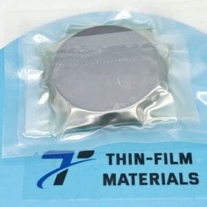
Selenium Sputtering Target Packaging

Our selenium sputter coater targets are clearly tagged and labeled externally to ensure efficient identification and quality control. We take great care to prevent any damage during storage and transportation, ensuring the targets remain in pristine condition.

Get Contact

TFM offers  Selenium  Sputtering Targets in various forms, purities, sizes, and prices. We specialize in high-purity thin film deposition materials with optimal density and minimal grain sizes, which are ideal for semiconductor, CVD, and PVD applications in display and optics. Contact Us for current pricing on sputtering targets and other deposition materials that are not listed.

Related Products

FAQ

It’s the source material (in solid form) used in sputter deposition to eject atoms or molecules that then form a thin film on a substrate.

Targets can be pure metals (e.g., gold, copper, aluminum), ceramics (e.g., Al₂O₃, SiO₂, TiO₂), alloys, or composites—chosen based on the film’s desired properties.


They are produced by processes such as melting/casting for metals or sintering (often with hot isostatic pressing) for ceramics and composite targets to ensure high density and purity.


In a vacuum chamber, a plasma (typically argon) bombards the target, ejecting atoms that travel and condense on a substrate, forming a thin film.


Key factors include the target’s purity, density, grain structure, and the sputtering yield (i.e. how many atoms are ejected per incident ion), as well as operating conditions like power density and gas pressure.


Operators monitor target erosion (often by measuring the depth of the eroded “race track”) or track total energy delivered (kilowatt-hours) until it reaches a threshold that can compromise film quality.


Fragile materials (such as many ceramics or certain oxides) and precious metals often require a backing plate to improve cooling, mechanical stability, and to allow thinner targets that reduce material costs.


DC sputtering is used for conductive targets, while RF sputtering is necessary for insulating targets (like many oxides) because it prevents charge buildup on the target’s surface.


In reactive sputtering, a reactive gas (e.g., oxygen or nitrogen) is introduced to form compound films on the substrate, but it may also “poison” the target surface if not carefully controlled.


Many manufacturers prefer to control raw material quality by sourcing their own powders; using external powders can risk impurities and inconsistent target properties.


Targets should be stored in clean, dry conditions (often in original packaging or re-wrapped in protective materials) and handled with gloves to avoid contamination, ensuring optimal performance during deposition.

Deposition rate depends on factors such as target material and composition, power density, working gas pressure, substrate distance, and the configuration of the sputtering system (e.g., magnetron design).

 
Shopping Cart