Silicon Carbide Sputtering Target
Introduction
The Silicon Carbide (SiC) Sputtering Target from Thin Film Materials (TFM) is a high-performance ceramic material widely used in semiconductors, optoelectronics, protective coatings, and energy devices. Silicon carbide is renowned for its exceptional hardness, wide bandgap, thermal conductivity, and chemical stability, making it a critical material for advanced thin film deposition.
Detailed Description
TFM’s SiC sputtering targets are manufactured with high density, fine grain structure, and purities ranging from 99.9% to 99.99%, ensuring uniform sputtering and stable film composition.
Chemical Formula: SiC
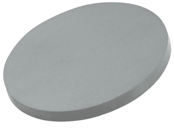
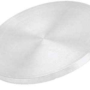
Appearance: Black to dark gray ceramic solid
Density: ~3.21 g/cm³
Melting Point: Sublimes above 2,700 °C
Crystal Structure: Hexagonal or cubic (polytypes such as 4H-SiC, 6H-SiC)
We provide SiC sputtering targets in standard disc, rectangular, and step target forms. Bonding services with indium or elastomer onto copper or titanium backing plates are available to improve heat dissipation and extend target lifetime. Custom dimensions and polytype selections can also be tailored to specific research or industrial requirements.
Applications
Silicon Carbide sputtering targets are widely applied in:
Semiconductor devices: thin films for high-power, high-frequency, and high-temperature electronics
Protective coatings: hard coatings with excellent wear and corrosion resistance
Optoelectronics: UV photodetectors, LEDs, and optical windows
Energy technologies: films for solar cells and thermal management components
Research: advanced studies in wide bandgap semiconductors and nanostructured coatings
Technical Parameters
| Parameter | Typical Value / Range | Importance |
|---|---|---|
| Purity | 99.9% – 99.99% | Ensures high-quality thin films with minimal contamination |
| Diameter | 25 – 150 mm (custom up to 300 mm) | Fits most commercial sputtering systems |
| Thickness | 3 – 6 mm | Influences sputtering rate and film thickness |
| Bonding Options | Indium / Elastomer | Improves adhesion, stability, and heat transfer |
| Backing Plate | Copper / Titanium | Enhances structural and thermal performance |
Comparison with Related Materials
| Material | Key Advantage | Typical Application |
|---|---|---|
| Silicon Carbide (SiC) | High hardness, wide bandgap, thermal stability | Power electronics, hard coatings |
| Silicon (Si) | Cost-effective semiconductor | Microelectronics, photovoltaics |
| Aluminum Nitride (AlN) | Excellent thermal conductivity | Substrates, optoelectronics |
FAQ
| Question | Answer |
|---|---|
| Can SiC sputtering targets be customized? | Yes, TFM provides custom diameters, thicknesses, polytypes, and bonded assemblies. |
| Do you offer bonding services? | Yes, indium and elastomer bonding with Cu/Ti backing plates are available. |
| How are the targets packaged? | Vacuum-sealed, protected with foam, and shipped in export-safe cartons or crates. |
| Which industries use SiC targets most? | Semiconductors, energy, protective coatings, aerospace, and research. |
Packaging
Each Silicon Carbide sputtering target is vacuum-sealed and securely packaged to protect against moisture, oxidation, and mechanical damage. Export-ready cartons or wooden crates ensure safe delivery worldwide.
Conclusion
The Silicon Carbide (SiC) Sputtering Target from TFM combines high purity, outstanding hardness, and superior thermal stability, making it an excellent choice for next-generation thin film applications. With customizable specifications and bonding options, our SiC targets provide reliable performance for both R&D and industrial-scale production.
For specifications, pricing, and custom solutions, please contact us at sales@thinfilmmaterials.com
Silicon Carbide Sputtering Target Bonding Services
Specialized bonding services for Silicon Carbide Sputtering Targets, including indium and elastomeric bonding techniques, enhance performance and durability. Thin Film Materials (TFM) ensures high-quality solutions that meet industry standards and customer needs.
We also offer custom machining of backing plates, which is essential for sputtering target assembly. This comprehensive approach improves target design flexibility and performance in thin film deposition. Our channels provide detailed information about bonding materials, methods, and services, helping clients make informed decisions.


Reviews
There are no reviews yet.