 MSDS File
Silicon Dioxide Evaporation Materials Overview
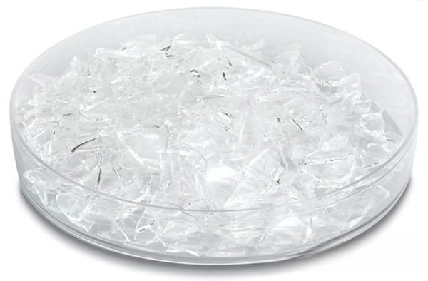
Silicon dioxide, chemically represented as SiO2, is a crucial material in the world of evaporation processes. With a melting point of 1,610°C, a density of 2.648 g/cc, and a vapor pressure of 10⁻⁴ Torr at 1,025°C, silicon dioxide is a highly stable compound. Naturally occurring as sand or quartz, this material is integral in manufacturing glass products, such as windows and bottles. For high-quality film deposition, silicon dioxide’s purity is essential, and our high-purity SiO2 evaporation materials, achieving up to 99.9995% purity, ensure excellent performance in these processes.
Silicon Dioxide Evaporation Materials Specification
| Material Type | Silicon Dioxide |
| Symbol | SiO2 |
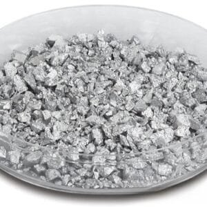
| Color/Appearance | White Solid |
| Melting Point | 1,713 °C (3,115 °F; 1,986 K) (amorphous) |
| Theoretical Density | 2.648 (α-quartz), 2.196 (amorphous) g·cm−3 |
| Purity | 99.9% ~ 99.995% |
| Shape | Powder/ Pellets/ Granule/ Custom-made |
Applications of Silicon Dioxide Evaporation Materials
Silicon dioxide evaporation materials are essential for various high-tech applications:
- Deposition Processes: Utilized in semiconductor deposition, chemical vapor deposition (CVD), and physical vapor deposition (PVD).
- Optical Applications: Employed in protective coatings, decorative finishes, and display technologies.
Packaging and Handling
To maintain product integrity, our silicon dioxide evaporation materials are carefully tagged and labeled. We ensure protection against damage during storage and transit, adhering to strict quality control measures.
Contact Us
As a premier supplier of high-purity silicon dioxide evaporation materials, we offer a variety of forms including tablets, granules, rods, and wires. Custom shapes and quantities can be tailored to meet specific needs. In addition to evaporation materials, we provide related products such as evaporation sources, boats, filaments, crucibles, heaters, and e-beam crucible liners. For current pricing and inquiries about materials not listed, please contact us.


Reviews
There are no reviews yet.