
 MSDS File
Introduction
Silicon Monoxide Evaporation Materials (SiO) are widely used in vacuum deposition systems for producing protective, optical, and barrier thin films. As a sub-oxide of silicon, SiO offers excellent adhesion, moderate refractive index, and reliable moisture barrier properties, making it a preferred material in optics, packaging, and electronic applications.
SiO has long been a standard material for thin film coatings in electron beam and thermal evaporation processes due to its stable evaporation characteristics and ability to form dense, uniform films under controlled vacuum conditions.
Detailed Description
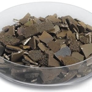
Silicon Monoxide (SiO) is a thermally evaporated oxide material with a melting/sublimation behavior suitable for high-vacuum deposition. It is commonly supplied in:
Irregular pieces
Granules
Pellets
Custom-shaped charges
High-purity grades (99.9% – 99.99%) are manufactured through controlled synthesis and purification processes to minimize metallic impurities and ensure consistent film properties.
Key material characteristics include:
Good adhesion to glass, polymers, and metal substrates
Moderate refractive index (~1.8–2.0 depending on deposition conditions)
Effective moisture and gas barrier performance
Chemical stability in dry environments
During evaporation, SiO can partially oxidize to form SiOₓ (where x ≈ 1.5–2.0), depending on oxygen availability and deposition parameters. Oxygen partial pressure control allows fine-tuning of film composition and optical performance.
SiO films are known for their dense microstructure and mechanical durability compared to some low-index fluoride materials.
Applications
Silicon Monoxide Evaporation Materials are widely used in:
Optical interference coatings
Protective overcoats on mirrors and lenses
Moisture barrier coatings on flexible packaging
Infrared optical films
Semiconductor device passivation layers
Organic electronics encapsulation
Decorative and functional thin films
In optical stacks, SiO is often used as an intermediate refractive index layer or protective coating.
Technical Parameters
| Parameter | Typical Value / Range | Importance |
|---|---|---|
| Chemical Formula | SiO | Defines sub-oxide evaporation behavior |
| Purity | 99.9% – 99.99% | Reduces contamination and defects |
| Form | Pieces / Granules / Pellets | Compatible with crucibles |
| Refractive Index | ~1.8–2.0 (film dependent) | Influences optical design |
| Deposition Method | Thermal / E-beam Evaporation | Ensures uniform thin film growth |
| Density (bulk) | ~2.1–2.2 g/cm³ | Relevant for rate control |
Custom sizes and packaging configurations are available based on deposition system requirements.
Comparison with Related Silicon Oxide Materials
| Material | Key Advantage | Typical Application |
|---|---|---|
| SiO | Good adhesion & barrier performance | Protective optical coatings |
| SiO₂ | Low refractive index | AR coatings & insulation |
| Al₂O₃ | Strong dielectric properties | Protective films |
| MgF₂ | Very low refractive index | Anti-reflective layers |
Compared to SiO₂, SiO offers better adhesion to certain substrates and is often easier to evaporate at lower temperatures.
FAQ
| Question | Answer |
|---|---|
| Is SiO suitable for thermal evaporation? | Yes, it is commonly used in both thermal and electron beam evaporation systems. |
| Can film stoichiometry be controlled? | Yes, oxygen partial pressure and deposition parameters influence SiOₓ composition. |
| Is it suitable for barrier coatings? | Yes, SiO films provide effective moisture and gas barrier performance. |
| Can custom pellet sizes be supplied? | Yes, material form and size can be tailored to your equipment. |
| Are certificates provided? | Yes, chemical analysis and batch traceability documentation are available. |
Packaging
Our Silicon Monoxide Evaporation Materials are meticulously tagged and labeled externally to ensure efficient identification and maintain high standards of quality control. Materials are vacuum-sealed or packed in moisture-resistant containers to maintain stability during storage and transportation.
Conclusion
Silicon Monoxide Evaporation Materials (SiO) offer a reliable solution for optical coatings, protective films, and barrier applications. With controlled purity, stable evaporation characteristics, and flexible customization options, they support both research and industrial thin film deposition processes.
For detailed specifications and a quotation, please contact us at sales@thinfilmmaterials.com.


Reviews
There are no reviews yet.