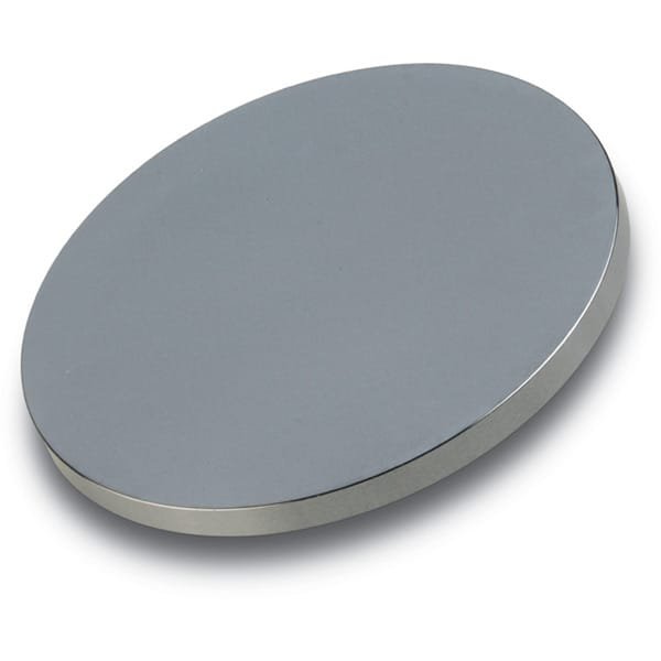

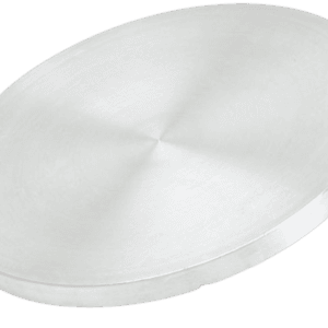
Silicon Sputtering Target Description
Silicon sputtering targets from TFM are high-purity elemental materials engineered for precision thin film deposition processes such as Physical Vapor Deposition (PVD), including magnetron sputtering. These targets are widely used in the semiconductor, solar, optics, and MEMS industries for the fabrication of advanced microelectronic components.
Silicon (Si) is a chemical element with the atomic number 14, positioned in Group 14 and Period 3 of the periodic table. It is the second most abundant element in the Earth’s crust and is widely valued for its semiconductor properties. Silicon’s symbol “Si” is derived from the Latin word “silex,” meaning flint. It has a relative atomic mass of 28.0855 and exists as a dark gray crystalline solid with a diamond cubic structure.
Silicon is a key material for integrated circuits, solar cells, and various dielectric and passivation layers. When used as a sputtering target, it enables precise and controlled deposition of thin silicon films on substrates such as glass, silicon wafers, and plastics.
Silicon Sputtering Target Specification
| Property | Value |
|---|---|
| Element Symbol | Si |
| Atomic Number | 14 |
| Molecular Weight | 28.09 g/mol |
| Appearance | Gray to dark gray solid |
| Melting Point | 1414 °C |
| Density | 2.33 g/cm³ |
| Purity | 99.9%, 99.99%, 99.999% (3N–5N) |
| Available Sizes | Dia.: 1″, 2″, 3″, 4″, 5″, 6″, 8″ Thick: 0.125″, 0.250″, custom sizes available |
Silicon Sputtering Target Handling Notes
Handle with care to prevent contamination; always use clean gloves or tweezers.
Silicon is brittle and should be supported properly during installation to avoid cracking.
For improved sputtering stability, backing plates or elastomer bonding may be applied.
Silicon Sputtering Target Packaging
TFM’s silicon sputtering targets are vacuum-sealed or double-bagged in cleanroom conditions, with all packaging materials clearly labeled for traceability and safe handling. We ensure that each target arrives undamaged and ready for high-performance deposition applications.
Get Contact
TFM offers a wide range of Silicon Sputtering Targets in various sizes, thicknesses, and purities to suit your deposition process. Whether for semiconductor research, solar cell manufacturing, or optical coatings, our silicon targets meet stringent quality standards for density, grain size, and uniformity.
Contact Us to request a quote or inquire about custom compositions and bonding services.


Reviews
There are no reviews yet.