
| Material Type | Terbium Ferrite |
| Symbol | Tb3Fe5O12 |
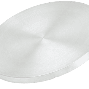
| Color/Appearance | Various colors, Solid |
| Melting Point (°C) | N/A |
| Theoretical Density (g/cc) | N/A |
| Water Solubility | Insoluble |
| Sputter | RF, RF-R, DC |
| Type of Bond | Indium, Elastomer |
Terbium Ferrite Sputtering Targets
TFM offers high-quality Terbium Ferrite Sputtering Targets (Tb₃Fe₅O₁₂), designed for thin-film deposition in various advanced applications, such as ferroelectrics, gate dielectrics, and CMOS technologies. Known for their exceptional Faraday effect properties, Terbium Ferrite materials are used in magneto-optic devices and data storage applications.
Key Features and Advantages
Purity: 99.9% – Ensures high-performance thin-film deposition, ideal for electronic and optical applications.
Custom Sizes Available – Tailored to meet specific requirements for research and industrial applications, ensuring versatility.
Superior Magnetic Properties – Offers magneto-optic behavior, beneficial in applications requiring high magnetic sensitivity.
Excellent Faraday Effect – The orientation dependence and field behavior at low temperatures make these targets unique in magneto-optical systems.
Stable Hysteresis Loop – Features minimal asymmetry near the compensation point for consistent device performance.
Durable & Reliable – Cold pressed, sintered, and elastomer bonded to a backing plate, ensuring consistent deposition performance in high-demand applications.
Specifications
Circular Targets:
Diameter ≤ 14 inches
Thickness ≥ 1mm
Block Targets:
Length ≤ 32 inches
Width ≤ 12 inches
Thickness ≥ 1mm
Applications
Ferroelectrics – Used in memory devices, capacitors, and actuators due to their excellent magnetic properties.
Gate Dielectric for CMOS – Ideal for CMOS technology, enabling high-efficiency gate dielectric layers.
Magneto-Optic Devices – Applied in data storage, optical switches, and sensor technologies.
Thin-Film Deposition – Used in advanced thin films for spintronic devices, optical coatings, and microwave devices.
Manufacturing Process
Manufacturing: Cold pressed and sintered to ensure high-density targets that meet stringent performance standards.
Bonding: Elastomer bonded to a backing plate for durability and ease of handling during sputtering.
Cleaning & Final Packaging: Thoroughly cleaned for vacuum applications and packaged to ensure protection from environmental contaminants during shipment.
Options
Custom Sizes Available – Targets can be made to fit specific customer requirements.
R&D Purposes – Smaller sizes are offered for research and development applications.
Sputtering Target Bonding Service – Enhance target performance and reliability with our sputtering target bonding service.
Industry Impact
TFM’s Terbium Ferrite Sputtering Targets provide a critical material for advanced semiconductor, optical, and ferroelectric applications. With high purity, outstanding magneto-optic properties, and customizable sizes, they are the preferred choice for industries that rely on high-performance thin films, such as data storage, CMOS manufacturing, and spintronic technology.


Reviews
There are no reviews yet.