
 MSDS File
Introduction
Thulium (Tm) is a heavy rare-earth element valued for its unique optical and electronic properties. In thin film deposition, Thulium Evaporation Materials are primarily used for physical vapor deposition (PVD) processes such as thermal evaporation and electron beam evaporation. With its narrow emission bands and compatibility with oxide and fluoride systems, thulium plays an important role in advanced photonics, infrared devices, specialty coatings, and research-grade thin films.
For laboratories and industrial coating lines requiring precise rare-earth doping or functional optical layers, high-purity thulium ensures stable evaporation behavior and consistent film composition.
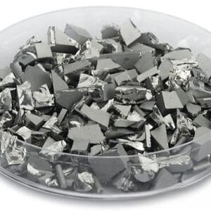
Detailed Description
Thulium Evaporation Materials are supplied in various forms including pieces, granules, pellets, and custom-shaped slugs to match different evaporation sources and crucible geometries. Typical purities range from 99.9% (3N) to 99.99% (4N), with controlled levels of oxygen and other rare-earth impurities.
As a rare-earth metal, thulium exhibits:
High melting point (~1545 °C), suitable for e-beam evaporation
Stable vapor pressure characteristics under high vacuum
Excellent compatibility with oxide formation (e.g., Tm₂O₃ thin films)
Narrow-band optical emission around 1.47–2.0 µm when incorporated in host matrices
In evaporation processes, material purity directly affects film transparency, defect density, and optical performance. Controlled granule size improves evaporation uniformity, while compact pellets reduce material spitting during heating. For research-scale deposition, smaller batch quantities are available; for production-scale coating, larger lots with consistent lot traceability can be supplied.
Thulium can also be used as a precursor for reactive deposition to form thulium oxide or doped functional films in oxygen atmospheres.
Applications
Thulium Evaporation Materials are widely used in:
Optical coatings for infrared transmission and specialty filters
Laser materials research, especially Tm-doped crystals and thin films
Infrared detectors and sensors
Photonic and waveguide structures
Functional oxide thin films (Tm₂O₃)
Advanced semiconductor and research coatings
Solid-state lighting and luminescent materials development
In research environments, thulium is frequently used for controlled doping of host matrices such as YAG, YLF, and various oxide substrates to tune emission properties.
Technical Parameters
| Parameter | Typical Value / Range | Importance |
|---|---|---|
| Purity | 99.9% – 99.99% | Higher purity improves optical clarity and reduces contamination |
| Form | Pieces, Granules, Pellets | Matches different evaporation source designs |
| Size | 1 – 10 mm (customizable) | Influences evaporation stability and loading efficiency |
| Melting Point | ~1545 °C | Determines suitable evaporation method |
| Density | ~9.32 g/cm³ | Relevant for weight calculation and deposition rate control |
| Recommended Method | Thermal / E-beam Evaporation | Ensures controlled thin film growth |
Custom sizes and tailored packaging are available to meet specific deposition system requirements.
Comparison with Related Rare Earth Materials
| Material | Key Advantage | Typical Application |
|---|---|---|
| Thulium (Tm) | Infrared emission characteristics | IR photonics & doped laser films |
| Erbium (Er) | 1.55 µm telecom emission | Optical fiber amplifiers |
| Ytterbium (Yb) | High efficiency laser doping | High-power solid-state lasers |
| Neodymium (Nd) | Strong visible/near-IR emission | Nd:YAG laser systems |
Compared with erbium and ytterbium, thulium is particularly suitable for mid-infrared applications and specialty laser research.
FAQ
| Question | Answer |
|---|---|
| Can Thulium Evaporation Materials be customized? | Yes, purity, form, size, and batch quantity can be tailored to your deposition system. |
| Is thulium suitable for thermal evaporation? | It can be used in thermal evaporation, but e-beam evaporation is generally preferred due to its melting point. |
| Can it be used for oxide film deposition? | Yes, reactive evaporation in oxygen atmosphere can produce Tm₂O₃ thin films. |
| How should the material be stored? | Store in a dry, inert environment to minimize surface oxidation. |
| Do you provide traceability documents? | Yes, material certificates and batch traceability are available upon request. |
Packaging
Our Thulium Evaporation Materials are meticulously tagged and labeled externally to ensure efficient identification and maintain high standards of quality control. We take great care to prevent any potential damage during storage and transportation, ensuring the materials arrive in excellent condition. Packaging options include vacuum-sealed bags with moisture barrier protection and shock-resistant export cartons.
Conclusion
Thulium Evaporation Materials provide a reliable solution for infrared photonics, functional oxide thin films, and rare-earth-doped research applications. With controlled purity, consistent evaporation behavior, and flexible customization options, they are well suited for both laboratory-scale research and industrial thin film production.
For detailed specifications and a quotation, please contact us at sales@thinfilmmaterials.com.


Reviews
There are no reviews yet.