
Introduction
Thulium Telluride Sputtering Target (TmTe) is a specialized compound target used in thin film deposition processes such as magnetron sputtering and other physical vapor deposition (PVD) technologies. As a rare-earth chalcogenide material, thulium telluride exhibits unique electronic, magnetic, and optical properties that make it valuable for advanced semiconductor research and functional thin film development.
TmTe sputtering targets are primarily used in research environments where rare-earth telluride compounds are investigated for their semiconducting behavior, infrared optical characteristics, and potential applications in quantum materials. Thin films deposited from TmTe targets enable the exploration of strongly correlated electronic systems, rare-earth magnetism, and advanced optoelectronic materials.
Detailed Description
Thulium Telluride (TmTe) is a rare-earth telluride compound composed of thulium (Tm), a lanthanide element, and tellurium (Te), a chalcogen. The compound crystallizes in a rock-salt type structure, which is common among many rare-earth chalcogenides. This crystal structure contributes to its distinctive electronic and magnetic characteristics, including semiconducting behavior and strong electron–electron interactions.
Producing TmTe sputtering targets requires careful synthesis and processing of high-purity raw materials. The compound is typically prepared through controlled reaction processes followed by powder consolidation techniques such as hot pressing or hot isostatic pressing (HIP). These methods allow manufacturers to produce dense targets with uniform microstructure, which is essential for stable sputtering performance and consistent thin film deposition.
Because rare-earth tellurides can be sensitive to oxidation, the manufacturing and handling of TmTe sputtering targets often take place under controlled atmospheres. Maintaining high chemical purity is critical for achieving reliable thin film properties, especially in electronic and optical applications where impurities may significantly affect device performance.
During sputtering, the TmTe target serves as the source material for depositing compound thin films that retain the stoichiometric ratio of thulium and tellurium. These films can exhibit interesting electrical and magnetic characteristics that are valuable in condensed matter physics research and advanced electronic materials development.
To improve thermal stability in sputtering systems, TmTe targets may be bonded to copper backing plates. This configuration enhances heat dissipation and allows the target to operate reliably under higher power densities.
Applications
Thulium Telluride Sputtering Targets are mainly used in specialized research and advanced materials development, including:
Semiconductor research involving rare-earth chalcogenide thin films
Infrared and optoelectronic materials where telluride compounds exhibit useful optical properties
Magnetic and strongly correlated materials studies in condensed matter physics
Quantum materials research exploring rare-earth electron interactions
Functional thin film development for experimental electronic devices
Advanced materials laboratories studying lanthanide-based semiconductors
Due to their unique electronic structure, rare-earth telluride films are particularly interesting for exploring new quantum and magnetic phenomena.
Technical Parameters
| Parameter | Typical Value / Range | Importance |
|---|---|---|
| Purity | 99.9% – 99.99% | High purity reduces contamination in deposited films |
| Composition | Stoichiometric TmTe | Ensures proper electronic and magnetic properties |
| Density | ≥ 95% theoretical density | Provides stable sputtering performance |
| Diameter | 25 – 300 mm (custom) | Compatible with various sputtering systems |
| Thickness | 3 – 6 mm | Affects target life and sputtering rate |
| Bonding | Copper backing plate optional | Improves thermal conductivity and structural stability |
Comparison with Related Materials
| Material | Key Advantage | Typical Application |
|---|---|---|
| Thulium Telluride (TmTe) | Rare-earth semiconductor with unique magnetic properties | Quantum materials research |
| Europium Telluride (EuTe) | Strong magnetic interactions | Magneto-optical materials |
| Lanthanum Telluride (LaTe) | Interesting electronic structure | Electronic and optical research |
| Tellurium (Te) | Good semiconductor properties | Photovoltaics and thermoelectrics |
FAQ
| Question | Answer |
|---|---|
| Can the Thulium Telluride Sputtering Target be customized? | Yes, the target size, thickness, purity level, and bonding configuration can be customized according to the deposition system. |
| Is TmTe suitable for semiconductor thin film research? | Yes, TmTe is commonly studied as a rare-earth semiconductor material with unique electronic and magnetic characteristics. |
| Do these targets require backing plates? | For high-power sputtering processes, copper backing plates are recommended to improve heat dissipation and target stability. |
| Which deposition methods can use TmTe targets? | RF magnetron sputtering and other PVD methods are commonly used for depositing rare-earth telluride films. |
| What industries or institutions use this material? | Primarily universities, research institutes, semiconductor laboratories, and advanced materials research centers. |
Packaging
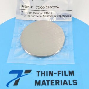
Our Thulium Telluride Sputtering Target are meticulously tagged and labeled externally to ensure efficient identification and maintain high standards of quality control. We take great care to prevent any potential damage during storage and transportation, ensuring the targets arrive in perfect condition.
Conclusion
Thulium Telluride Sputtering Targets provide a reliable source material for depositing rare-earth telluride thin films with unique electronic, magnetic, and optical properties. These targets are particularly valuable in semiconductor research, condensed matter physics, and advanced optoelectronic materials development.
With customizable dimensions, high purity options, and reliable bonding configurations, TmTe sputtering targets support the demanding requirements of modern thin film research and deposition systems.
For detailed specifications and a quotation, please contact us at sales@thinfilmmaterials.com.


Reviews
There are no reviews yet.