Introduction
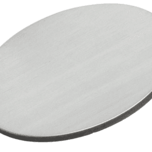
The Tin Antimonide Sputtering Target (SnSb) is a compound alloy target widely used in thin-film deposition for phase-change materials, thermoelectric research, and advanced electronic devices. By combining tin (Sn) and antimony (Sb), SnSb enables the deposition of films with controllable electrical resistivity, crystallization behavior, and thermal stability—key requirements in modern data storage, memory devices, and functional thin-film applications.
SnSb sputtering targets are especially valued in research and pilot-scale production environments where precise stoichiometry and reproducible sputtering performance are essential.
Detailed Description
Tin Antimonide sputtering targets are manufactured from high-purity tin and antimony raw materials using controlled melting, alloying, and precision machining processes. The resulting target exhibits uniform composition, stable microstructure, and consistent density—factors that directly influence sputtering rate stability and film uniformity.
SnSb targets can be supplied in various atomic or weight ratios depending on application requirements, allowing fine control over phase-change temperature, electrical conductivity, and optical contrast in deposited films. During magnetron sputtering, SnSb demonstrates stable plasma interaction and predictable target erosion behavior, making it suitable for both R&D and small-to-medium production runs.
Targets are available as monolithic alloy discs or bonded to copper or titanium backing plates to improve heat dissipation and power handling, particularly under higher sputtering power conditions.
Applications
Tin Antimonide sputtering targets are commonly used in:
Phase-change memory (PCM) and data storage research
Thermoelectric thin films and devices
Semiconductor and electronic materials development
Infrared and optoelectronic coatings
Functional alloy thin films
Academic and industrial thin-film R&D
Technical Parameters
| Parameter | Typical Value / Range | Importance |
|---|---|---|
| Chemical Composition | Sn–Sb (custom ratios available) | Controls electrical & phase behavior |
| Purity | 99.9% – 99.99% | Improves film consistency |
| Target Diameter | 25 – 300 mm (custom) | Compatible with standard guns |
| Thickness | 3 – 6 mm (custom) | Influences sputtering stability |
| Density | ≥ 99% of theoretical | Ensures uniform erosion |
| Backing Plate | Optional (Cu / Ti) | Enhances thermal management |
| Deposition Method | DC / RF Magnetron Sputtering | Process flexibility |
Comparison with Related Sputtering Targets
| Material | Key Advantage | Typical Application |
|---|---|---|
| Tin Antimonide (SnSb) | Tunable phase-change behavior | Memory & thermoelectrics |
| Germanium Antimony Telluride (GST) | Fast phase switching | PCM devices |
| Antimony Telluride (Sb₂Te₃) | Thermoelectric efficiency | IR & TE devices |
| Tin Telluride (SnTe) | Narrow bandgap semiconductor | Infrared applications |
FAQ
| Question | Answer |
|---|---|
| Can the Sn/Sb ratio be customized? | Yes, composition can be tailored to specific research or process needs. |
| Is bonding recommended? | Bonded targets are recommended for higher power or larger diameters. |
| Is DC sputtering suitable? | Yes, DC sputtering is commonly used for SnSb alloy targets. |
| Are small research targets available? | Yes, lab-scale diameters and thicknesses are supported. |
| How is the target packaged? | Vacuum-sealed with protective cushioning for safe delivery. |
Packaging
Our Tin Antimonide Sputtering Targets are meticulously tagged and labeled for accurate identification and quality traceability. Each target is vacuum-sealed and protected with anti-static and shock-absorbing materials to prevent contamination or mechanical damage during storage and transportation. Export-grade cartons or wooden crates are used when required.
Conclusion
The Tin Antimonide Sputtering Target (SnSb) provides a reliable material solution for depositing phase-change and functional alloy thin films with controlled electrical and thermal properties. With customizable composition, stable sputtering behavior, and dependable quality, SnSb targets are an excellent choice for advanced thin-film research and electronic material development.
For detailed specifications and a quotation, please contact us at sales@thinfilmmaterials.com.


Reviews
There are no reviews yet.