
 MSDS File
| Material Type | Tin Arsenic |
| Symbol | SnAs |
| Melting Point (°C) | |
| Theoretical Density (g/cc) |
| Z Ratio | |
| E-Beam | |
| E-Beam Crucible Liner Material | |
| Temp. (°C) for Given Vap. Press. (Torr) | |
| Comments |
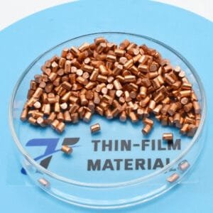
Tin Arsenic Pellet Evaporation Material (SnAs)
TFM offers high-quality Tin Arsenic Pellet Evaporation Material engineered for precise thin-film deposition in advanced semiconductor and optoelectronic applications. This material, composed of tin (Sn) and arsenic (As), is valued for its unique electrical and optical properties, robust chemical stability, and excellent thermal performance. The evaporation process using Tin Arsenic Pellet Evaporation Material ensures the production of uniform, defect-free thin films with precise thickness control and low impurity levels.
The exceptional characteristics of Tin Arsenic Pellet Evaporation Material make it ideal for a variety of high-performance applications. Its superior electrical conductivity and excellent optical absorption properties are critical for the fabrication of integrated circuits, photodetectors, solar cells, and infrared sensors. Additionally, the material’s stable chemical composition and robust thermal properties ensure reliable performance even under high-temperature processing and in harsh operating environments.
During the evaporation process, careful control of parameters such as deposition rate, ambient pressure, and substrate temperature guarantees optimal film formation. This results in films with enhanced adhesion, uniform density, and consistent performance, meeting the stringent requirements of modern thin-film technologies. TFM’s Tin Arsenic Pellet Evaporation Material is produced using advanced manufacturing techniques that allow for fine-tuning of the Sn:As ratio, thereby tailoring the material’s properties to specific application needs.
Whether used in research laboratories or industrial-scale production, Tin Arsenic Pellet Evaporation Material delivers outstanding reproducibility and reliability. Its ability to form high-quality films with excellent electrical and optical performance makes it indispensable for next-generation semiconductor devices and optoelectronic systems. TFM’s commitment to precision and quality ensures that this material remains at the forefront of innovation in the thin-film deposition industry, driving advancements in high-tech applications across various sectors.


Reviews
There are no reviews yet.