Generic selectors
Exact matches only
Search in title
Search in content
Post Type Selectors

ST0287 Tin (II) Sulfide Sputtering Target, SnS

Chemical Formula: SnS2
Catalog Number: ST0287
CAS Number: 1315-01-1
Purity: 99.9%
Shape: Discs, Plates, Column Targets, Step Targets, Custom-made

tin (II) sulfide sputtering target  come in various forms, purities, sizes, and prices. Thin Film Materials (TFM) manufactures and supplies top-quality sputtering targets at competitive prices.

Tin (II) Sulfide Sputtering Target Description

The Tin (II) Sulfide sputtering target is a type of sulfide ceramic sputtering target composed of tin and sulfur, specifically in the form of tin (II) sulfide (SnS). This material is commonly used in various industrial applications, particularly in the production of thin films through sputtering processes. These thin films are utilized in a range of applications including semiconductors, photovoltaic devices, and other advanced technological components.

Tin(II) chloride - Wikipedia

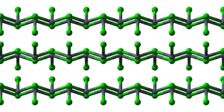
Tin (II) Sulfide (SnS) is a compound composed of tin and sulfur. It is typically found as a dark brown or black solid and is insoluble in water but can dissolve in concentrated hydrochloric acid. This material features a layered structure similar to that of black phosphorus, allowing it to be exfoliated into ultrathin flakes using ultrasonic methods in a liquid medium. These exfoliated SnS flakes possess a wider optical band gap, greater than 1.5 eV, compared to bulk crystals, making them potentially useful in various semiconductor applications, including photovoltaics and optoelectronic devices.


Related Product: Tin Sputtering Target

Tin (II) Sulfide Sputtering Target Specification

Compound FormulaSnS
AppearanceDark brown solid
Melting Point882 °C
Density5.22 g/cm3
Available SizesDia.: 1.0″, 2.0″, 3.0″, 4.0″, 5.0″, 6.0″
Thick: 0.125″, 0.250″

Tin (II) Sulfide Sputtering Target Application

The tin (II) sulfide sputtering target is widely utilized in various applications, including thin film deposition, decoration, semiconductor, display, LED, and photovoltaic devices. It is also employed in creating functional coatings and is used in industries such as optical information storage, glass coating (e.g., car glass and architectural glass), and optical communication. The material’s unique properties, such as its optical band gap and layer-structured semiconductor nature, make it suitable for these diverse applications, enhancing both the performance and functionality of the products it is used in.

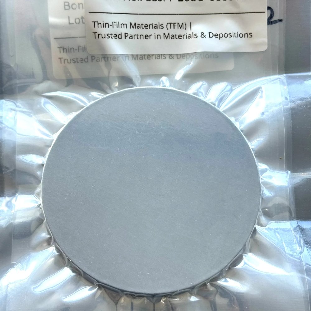
Tin (II) Sulfide Sputtering Target Packing

Our tin (II) sulfide sputter targets are meticulously tagged and labeled externally to guarantee efficient identification and maintain high standards of quality control. Special care is taken during storage and transportation to prevent any damage, ensuring that the products arrive in pristine condition for optimal use in various applications.

Get Contact

TFM offers tin (II) sulfide Sputtering Targets in various forms, purities, sizes, and prices. We specialize in high-purity thin film deposition materials with optimal density and minimal grain sizes, which are ideal for semiconductor, CVD, and PVD applications in display and optics. Contact Us for current pricing on sputtering targets and other deposition materials that are not listed.

Reviews

There are no reviews yet.

Be the first to review “ST0287 Tin (II) Sulfide Sputtering Target, SnS”

Your email address will not be published. Required fields are marked *

Related Products

FAQ

It’s the source material (in solid form) used in sputter deposition to eject atoms or molecules that then form a thin film on a substrate.

Targets can be pure metals (e.g., gold, copper, aluminum), ceramics (e.g., Al₂O₃, SiO₂, TiO₂), alloys, or composites—chosen based on the film’s desired properties.


They are produced by processes such as melting/casting for metals or sintering (often with hot isostatic pressing) for ceramics and composite targets to ensure high density and purity.


In a vacuum chamber, a plasma (typically argon) bombards the target, ejecting atoms that travel and condense on a substrate, forming a thin film.


Key factors include the target’s purity, density, grain structure, and the sputtering yield (i.e. how many atoms are ejected per incident ion), as well as operating conditions like power density and gas pressure.


Operators monitor target erosion (often by measuring the depth of the eroded “race track”) or track total energy delivered (kilowatt-hours) until it reaches a threshold that can compromise film quality.


Fragile materials (such as many ceramics or certain oxides) and precious metals often require a backing plate to improve cooling, mechanical stability, and to allow thinner targets that reduce material costs.


DC sputtering is used for conductive targets, while RF sputtering is necessary for insulating targets (like many oxides) because it prevents charge buildup on the target’s surface.


In reactive sputtering, a reactive gas (e.g., oxygen or nitrogen) is introduced to form compound films on the substrate, but it may also “poison” the target surface if not carefully controlled.


Many manufacturers prefer to control raw material quality by sourcing their own powders; using external powders can risk impurities and inconsistent target properties.


Targets should be stored in clean, dry conditions (often in original packaging or re-wrapped in protective materials) and handled with gloves to avoid contamination, ensuring optimal performance during deposition.

Deposition rate depends on factors such as target material and composition, power density, working gas pressure, substrate distance, and the configuration of the sputtering system (e.g., magnetron design).

 
Shopping Cart
Scroll to Top