
 MSDS File
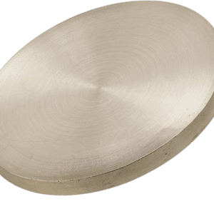
Titanium Fluoride Sputtering Target Target
The Titanium Fluoride Sputtering Target is a fluoride ceramic sputtering target composed of titanium and fluorine. It is specifically designed for use in various thin film deposition processes, among other industrial applications.
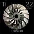 Titanium, represented by the chemical symbol “Ti,” is a chemical element named after the Titans, the powerful deities from Greek mythology. It was first discovered in 1791 by W. Gregor, with its isolation later accomplished and announced by J. Berzelius. Titanium has an atomic number of 22 and is located in Period 4 and Group 4 of the periodic table, within the d-block. The relative atomic mass of titanium is approximately 47.867(1) Dalton, with the number in parentheses indicating the uncertainty of this measurement.
Related Product: Titanium Sputtering Target
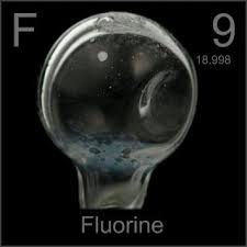 Fluorine, also known as fluorin, is a chemical element with the symbol “F.” Its name is derived from the Latin word ‘fluere,’ which means to flow. The element was first noted in 1810 by A.-M. Ampère, with its successful isolation later achieved by H. Moissan. Fluorine has an atomic number of 9 and is situated in Period 2 and Group 17 of the periodic table, falling within the p-block. The relative atomic mass of fluorine is 18.9984032(5) Dalton, with the number in brackets indicating the uncertainty of this measurement.
Titanium Fluoride Sputtering Target Application
The Titanium Fluoride Sputtering Target is widely utilized in various industrial applications. It is primarily used in thin film deposition processes, which are crucial for producing semiconductors, displays, LEDs, and photovoltaic devices. Additionally, it plays a significant role in decorative applications and functional coatings. This target is also used in the optical information storage industry, as well as in the glass coating industry for automotive and architectural glass, and in optical communication technologies.
Titanium Fluoride Sputtering Target Packing
Our Titanium Fluoride Sputter Targets are carefully tagged and labeled externally to ensure efficient identification and maintain rigorous quality control. We take meticulous precautions to prevent any damage during storage or transportation, ensuring the targets arrive in perfect condition.
Get Contact
TFM offers Titanium Fluoride Sputtering Targets in various forms, purities, sizes, and prices. We specialize in high-purity thin film deposition materials with optimal density and minimal grain sizes, which are ideal for semiconductor, CVD, and PVD applications in display and optics. Contact Us for current pricing on sputtering targets and other deposition materials that are not listed.


Reviews
There are no reviews yet.