Generic selectors
Exact matches only
Search in title
Search in content
Post Type Selectors

VD0653 Titanium Nickel Evaporation Materials, Ti/Ni

Catalog No.VD0653
MaterialTitanium Nickel (Ti/Ni)
Purity99.9% ~ 99.99%
ShapePowder/ Granule/ Custom-made

TFM is a prominent manufacturer and supplier of high-purity titanium nickel evaporation materials. Our extensive range includes materials in both powder and granule forms. We also provide custom options to meet specific needs, ensuring top-quality performance and versatility for your applications.

Titanium Nickel Evaporation Materials Description

Our titanium nickel evaporation materials are high-purity alloys composed of titanium (Ti) and nickel (Ni). These materials, which can reach up to 99.9995% purity, are essential for achieving high-quality thin films in various deposition processes. TFM is dedicated to producing these materials with stringent quality assurance to ensure exceptional reliability and performance.

Applications of Titanium Nickel Evaporation Materials

Titanium nickel evaporation materials are versatile and used in numerous applications, including:

  • Deposition Processes: Ideal for semiconductor deposition, chemical vapor deposition (CVD), and physical vapor deposition (PVD), these materials are critical for producing high-quality films.
  • Optical Coatings: Suitable for wear-resistant coatings, decorative finishes, and display technologies, they enhance both functionality and aesthetics.

Packaging and Handling

Our titanium nickel evaporation materials are carefully tagged and labeled to facilitate efficient identification and quality control. We take meticulous care to prevent any damage during storage and transportation.

Get in Touch

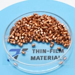
TFM is a leading supplier of high-purity titanium nickel evaporation materials, available in various forms such as tablets, granules, rods, and wires. Custom shapes and quantities can be provided upon request. In addition to evaporation materials, we offer evaporation sources, boats, filaments, crucibles, heaters, and e-beam crucible liners. For current pricing and inquiries about materials not listed, please contact us directly.

Reviews

There are no reviews yet.

Be the first to review “VD0653 Titanium Nickel Evaporation Materials, Ti/Ni”

Your email address will not be published. Required fields are marked *

FAQ

  • They are high‐purity substances (e.g. metals, alloys, or compounds) used in thermal or electron‐beam evaporation processes to form thin films on substrates.

  • Typically, they’re processed into a form (often ingots, pellets, or wires) that can be efficiently vaporized. Preparation emphasizes high purity and controlled composition to ensure film quality.

  • Thermal evaporation and electron-beam (e-beam) evaporation are the two main techniques, where material is heated (or bombarded with electrons) until it vaporizes and then condenses on the substrate.

  • Thermal evaporation heats the material directly (often using a resistive heater), while e-beam evaporation uses a focused electron beam to locally heat and vaporize the source material—each method offering different control and energy efficiency.

  • Key parameters include source temperature, vacuum level, deposition rate, substrate temperature, and the distance between the source and the substrate. These factors influence film uniformity, adhesion, and microstructure.

  • Evaporation generally produces high-purity films with excellent control over thickness, and it is especially suitable for materials with relatively low melting points or high vapor pressures.

  • Challenges include issues with step coverage (due to line-of-sight deposition), shadowing effects on complex topographies, and possible re-evaporation of material from the substrate if temperature isn’t properly controlled.

  • Common evaporation materials include noble metals (e.g., gold, silver), semiconductors (e.g., silicon, germanium), metal oxides, and organic compounds—each chosen for its specific optical, electrical, or mechanical properties.

  • Selection depends on desired film properties (conductivity, optical transparency, adhesion), compatibility with the evaporation process, and the final device application (semiconductor, optical coating, etc.).

  • Optimizing substrate temperature, deposition rate, and chamber vacuum are critical for ensuring that the film adheres well and forms the intended microstructure without defects.

  • Troubleshooting may involve checking the source material’s purity, ensuring stable source temperature, verifying the vacuum level, adjusting the substrate’s position or temperature, and monitoring deposition rate fluctuations.

While evaporation tends to yield very high purity films with excellent thickness control, it is limited by its line-of-sight nature. In contrast, sputtering can deposit films more uniformly on complex surfaces and is more versatile for a broader range of materials.


Shopping Cart
Scroll to Top