
Introduction
Titanium Tungsten Sputtering Target (Ti/W) is a widely used alloy target in thin film deposition processes such as magnetron sputtering and other physical vapor deposition (PVD) techniques. This alloy combines the excellent adhesion properties of titanium with the high density, thermal stability, and corrosion resistance of tungsten. As a result, Ti/W thin films are commonly employed as barrier layers, adhesion layers, and protective coatings in semiconductor manufacturing and advanced electronic devices.
Ti/W sputtering targets are especially important in integrated circuit fabrication, where thin films must provide reliable electrical performance while preventing metal diffusion between layers. The Ti/W alloy has become a standard material for diffusion barrier applications in microelectronics due to its stability and compatibility with various deposition systems.
Detailed Description
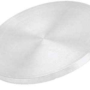
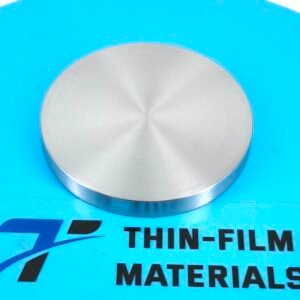
Titanium Tungsten (Ti/W) sputtering targets are manufactured from carefully controlled alloy compositions, typically containing tungsten as the primary component with a smaller percentage of titanium (commonly around Ti10W90 or Ti20W80 by weight). This composition provides an optimal balance between tungsten’s excellent barrier properties and titanium’s ability to improve adhesion to substrates such as silicon, silicon dioxide, and other semiconductor materials.
The manufacturing process generally involves vacuum melting or powder metallurgy techniques followed by hot pressing or hot isostatic pressing (HIP) to achieve a dense and homogeneous alloy structure. A uniform microstructure is essential for ensuring stable sputtering performance, minimizing particle generation, and maintaining consistent deposition rates across the substrate.
One of the most important characteristics of Ti/W thin films is their ability to function as an effective diffusion barrier. In semiconductor devices, these films prevent metal atoms—such as copper or aluminum—from diffusing into surrounding layers, which could otherwise degrade device performance. Ti/W films also exhibit excellent adhesion and good electrical conductivity, making them ideal for multilayer thin film structures.
For high-power sputtering systems, Titanium Tungsten targets are frequently bonded to copper backing plates using indium bonding or diffusion bonding techniques. These bonding methods improve heat dissipation and mechanical stability, allowing the targets to operate reliably during long deposition runs.
High-purity Ti/W targets are particularly important for semiconductor fabrication, where even trace impurities can affect thin film performance and device reliability.
Applications
Titanium Tungsten Sputtering Targets are widely used in advanced electronic and thin film applications, including:
Semiconductor device fabrication – Diffusion barrier layers in integrated circuits
Adhesion layers between metal films and semiconductor substrates
Thin film resistors and electronic components
Microelectromechanical systems (MEMS) requiring stable conductive coatings
Protective coatings with high thermal and chemical stability
Advanced research and development in thin film electronics and materials science
These applications benefit from the excellent thermal stability and barrier properties of Ti/W alloy films.
Technical Parameters
| Parameter | Typical Value / Range | Importance |
|---|---|---|
| Purity | 99.9% – 99.99% | Reduces contamination and improves thin film quality |
| Composition Ratio | Ti/W customizable (e.g., 10/90, 20/80) | Determines adhesion and barrier performance |
| Density | ≥ 99% theoretical density | Ensures stable sputtering and uniform deposition |
| Diameter | 25 – 300 mm (custom) | Compatible with most sputtering systems |
| Thickness | 3 – 6 mm | Influences target lifetime and sputtering rate |
| Bonding | Copper backing plate optional | Improves thermal conductivity and mechanical stability |
Comparison with Related Materials
| Material | Key Advantage | Typical Application |
|---|---|---|
| Titanium Tungsten (Ti/W) | Excellent diffusion barrier and adhesion | Semiconductor barrier layers |
| Titanium (Ti) | Strong adhesion to many substrates | Adhesion layers in thin films |
| Tungsten (W) | High melting point and density | High-temperature coatings |
| Tantalum (Ta) | Effective diffusion barrier for copper | Semiconductor interconnect structures |
FAQ
| Question | Answer |
|---|---|
| Can the Titanium Tungsten Sputtering Target be customized? | Yes, the Ti/W composition ratio, target size, thickness, purity, and bonding options can all be customized. |
| What is the most common Ti/W composition? | One of the most commonly used compositions is Ti10W90, which offers excellent diffusion barrier performance and adhesion. |
| Do Ti/W targets require backing plates? | For high-power sputtering systems, copper backing plates are recommended to improve heat dissipation and prevent thermal stress. |
| Which deposition methods are suitable for Ti/W targets? | Titanium Tungsten targets are typically used in DC magnetron sputtering and RF sputtering systems. |
| Which industries commonly use Ti/W sputtering targets? | Semiconductor manufacturing, MEMS fabrication, electronics production, and advanced materials research. |
Packaging
Our Titanium Tungsten Sputtering Target are meticulously tagged and labeled externally to ensure efficient identification and maintain high standards of quality control. We take great care to prevent any potential damage during storage and transportation, ensuring the targets arrive in perfect condition.
Conclusion
Titanium Tungsten Sputtering Targets are an essential material for depositing thin films that require strong adhesion, high thermal stability, and effective diffusion barrier properties. Their proven reliability in semiconductor fabrication makes them a standard choice for integrated circuits and advanced electronic devices.
With customizable alloy compositions, high purity levels, and robust bonding options, Ti/W sputtering targets are designed to meet the demanding requirements of modern vacuum deposition systems.
For detailed specifications and a quotation, please contact us at sales@thinfilmmaterials.com.

Reviews
There are no reviews yet.