Introduction
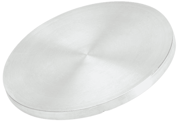
The Tungsten Boride (WB) Sputtering Target is a high-performance ceramic target used in advanced thin film deposition processes where exceptional hardness, thermal stability, and chemical resistance are required. Tungsten boride compounds belong to a class of ultra-hard materials that combine the refractory properties of tungsten with the strong covalent bonding characteristics of boron.
In Physical Vapor Deposition (PVD) systems such as RF magnetron sputtering, tungsten boride targets enable the deposition of durable thin films with excellent mechanical strength and wear resistance. These coatings are widely studied for applications in protective coatings, microelectronics, cutting tools, and high-temperature components where conventional metallic coatings may not provide sufficient durability.
Detailed Description
Tungsten Boride Sputtering Targets are typically produced using high-purity tungsten and boron powders through advanced powder metallurgy processes. These processes may include mechanical alloying, hot pressing, or hot isostatic pressing (HIP), followed by precision machining to produce dense ceramic targets with uniform microstructure.
Tungsten boride compounds exhibit remarkable physical and chemical characteristics, including:
Extremely high hardness comparable to superhard ceramics
High melting temperature and thermal stability
Excellent wear resistance
Strong chemical and oxidation resistance
Good electrical conductivity compared with many ceramics
These properties make tungsten boride thin films particularly suitable for demanding environments involving high friction, high temperature, or aggressive chemical exposure.
Due to its ceramic-like nature, the WB sputtering target is typically used with RF magnetron sputtering systems to ensure stable plasma generation and consistent deposition behavior. In some cases, DC sputtering may also be used if sufficient electrical conductivity is present.
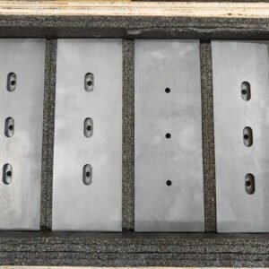
Tungsten boride targets can be manufactured in various geometries such as circular discs, rectangular plates, or custom shapes to match different sputtering cathodes. For high-power deposition systems or larger target diameters, the targets may be bonded to copper backing plates using indium bonding or elastomer bonding to improve thermal conductivity and structural stability.
High-density targets help ensure stable sputtering rates, reduced particle generation, and uniform film formation during deposition.
Applications
Thin films deposited from Tungsten Boride Sputtering Targets are used in several advanced industrial and research applications:
Wear-resistant coatings – ultra-hard coatings for cutting tools and mechanical components.
Protective coatings – thin films that resist abrasion, oxidation, and chemical corrosion.
Microelectronics – durable conductive coatings for semiconductor components.
High-temperature coatings – materials capable of maintaining stability in extreme thermal environments.
Aerospace materials research – advanced protective coatings for high-performance components.
Tribological coatings – low-friction and wear-resistant surfaces in precision mechanical systems.
Technical Parameters
| Parameter | Typical Value / Range | Importance |
|---|---|---|
| Purity | 99.5% – 99.9% | Higher purity improves film stability and hardness |
| Density | ≥95% theoretical | Ensures stable sputtering and consistent deposition |
| Diameter | 25 – 300 mm (custom) | Compatible with various sputtering cathodes |
| Thickness | 3 – 6 mm | Influences sputtering rate and target lifetime |
| Bonding | Copper backing plate (optional) | Improves heat dissipation and mechanical stability |
Comparison with Related Materials
| Material | Key Advantage | Typical Application |
|---|---|---|
| Tungsten Boride (WB) | Ultra-hard and wear-resistant | Protective coatings and cutting tools |
| Tungsten Carbide (WC) | Excellent hardness and toughness | Wear-resistant coatings and tooling |
| Titanium Nitride (TiN) | Decorative gold color with high hardness | Cutting tools and decorative coatings |
FAQ
| Question | Answer |
|---|---|
| Can tungsten boride sputtering targets be customized? | Yes, target dimensions, thickness, density, and backing plate bonding can be customized according to sputtering system requirements. |
| Which sputtering method is recommended for WB targets? | RF magnetron sputtering is typically used because tungsten boride behaves as a ceramic compound. |
| Are bonded targets available? | Yes, WB targets can be indium-bonded or elastomer-bonded to copper backing plates to improve thermal management. |
| What substrates are compatible with tungsten boride thin films? | Silicon wafers, steel substrates, ceramics, and other engineering materials are commonly used. |
| Which industries commonly use WB sputtering targets? | Semiconductor manufacturing, cutting tool coatings, aerospace materials research, and advanced tribological coating industries. |
Packaging
Our Tungsten Boride Sputtering Targets are meticulously tagged and labeled externally to ensure efficient identification and maintain strict quality control standards. Each target is vacuum-sealed and packed with protective cushioning materials to prevent contamination or mechanical damage during storage and transportation. Export-grade cartons or wooden crates are used to ensure safe international delivery.
Conclusion
The Tungsten Boride (WB) Sputtering Target is a high-performance ceramic target designed for the deposition of ultra-hard and wear-resistant thin films. Its exceptional hardness, thermal stability, and chemical resistance make it an ideal material for protective coatings, high-temperature components, and advanced tribological applications.
With high purity, customizable dimensions, and reliable manufacturing processes, tungsten boride sputtering targets provide consistent performance for both research laboratories and industrial thin film deposition systems.
For detailed specifications and a quotation, please contact us at sales@thinfilmmaterials.com.


Reviews
There are no reviews yet.