Generic selectors
Exact matches only
Search in title
Search in content
Post Type Selectors

VD0587 Tungsten Evaporation Materials, W

Catalog No.VD0587
MaterialTungsten (W)
Purity99.9% ~ 99.95%
ShapePowder/ Granule/ Custom-made

TFM is a leading manufacturer and supplier of high-purity tungsten evaporation materials, as well as a diverse range of other evaporation materials. We offer these materials in both powder and granule forms, and customized options are available upon request.

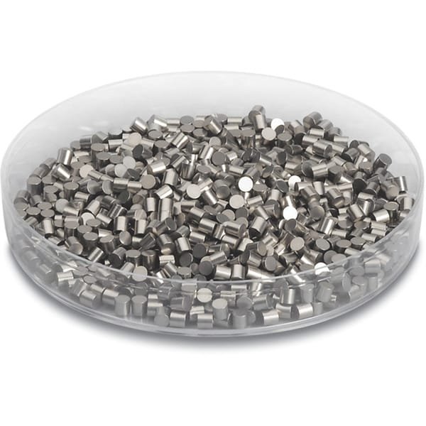
Tungsten Evaporation Materials Description

Tungsten is a rare metal that is primarily found in nature as part of chemical compounds rather than in its pure form. It was recognized as a new element in 1781 and first isolated as a metal in 1783. Key ores of tungsten include wolframite and scheelite. During the evaporation process, tungsten can form alloys with materials such as aluminum (Al) or gold (Au).

High-purity tungsten evaporation materials are essential for ensuring high-quality film deposition. TFM specializes in producing tungsten evaporation materials with up to 99.95% purity, employing stringent quality assurance practices to ensure product reliability.

Tungsten Evaporation Materials Specification

Material TypeTungsten
SymbolW
Color/AppearanceGrayish White, Lustrous, Metallic
Melting Point3410°C
Density19.3 g/cm3
Thermal Conductivity174 W/m.K
Melting Point3,410 °C
SynonymsTungsten Pellets, Tungsten Pieces, Tungsten Evaporation Pellet, W Pellets, W Pieces, W Evaporation Pellet

Tungsten Evaporation Materials Applications

  • Deposition Processes: Used in semiconductor deposition, chemical vapor deposition (CVD), and physical vapor deposition (PVD).
  • Optics: Applied in wear protection, decorative coatings, and displays.

Tungsten Evaporation Materials Packaging

Our tungsten evaporation materials are carefully handled to prevent damage during storage and transportation, ensuring they retain their original quality.

Contact Us

TFM offers tungsten evaporation materials in various forms, purities, sizes, and price ranges. We are dedicated to producing high-purity e-beam evaporation materials with the highest possible density and smallest average grain sizes. For current pricing on evaporation pellets and other deposition materials not listed, please contact us with your inquiry.

Reviews

There are no reviews yet.

Be the first to review “VD0587 Tungsten Evaporation Materials, W”

Your email address will not be published. Required fields are marked *

FAQ

  • They are high‐purity substances (e.g. metals, alloys, or compounds) used in thermal or electron‐beam evaporation processes to form thin films on substrates.

  • Typically, they’re processed into a form (often ingots, pellets, or wires) that can be efficiently vaporized. Preparation emphasizes high purity and controlled composition to ensure film quality.

  • Thermal evaporation and electron-beam (e-beam) evaporation are the two main techniques, where material is heated (or bombarded with electrons) until it vaporizes and then condenses on the substrate.

  • Thermal evaporation heats the material directly (often using a resistive heater), while e-beam evaporation uses a focused electron beam to locally heat and vaporize the source material—each method offering different control and energy efficiency.

  • Key parameters include source temperature, vacuum level, deposition rate, substrate temperature, and the distance between the source and the substrate. These factors influence film uniformity, adhesion, and microstructure.

  • Evaporation generally produces high-purity films with excellent control over thickness, and it is especially suitable for materials with relatively low melting points or high vapor pressures.

  • Challenges include issues with step coverage (due to line-of-sight deposition), shadowing effects on complex topographies, and possible re-evaporation of material from the substrate if temperature isn’t properly controlled.

  • Common evaporation materials include noble metals (e.g., gold, silver), semiconductors (e.g., silicon, germanium), metal oxides, and organic compounds—each chosen for its specific optical, electrical, or mechanical properties.

  • Selection depends on desired film properties (conductivity, optical transparency, adhesion), compatibility with the evaporation process, and the final device application (semiconductor, optical coating, etc.).

  • Optimizing substrate temperature, deposition rate, and chamber vacuum are critical for ensuring that the film adheres well and forms the intended microstructure without defects.

  • Troubleshooting may involve checking the source material’s purity, ensuring stable source temperature, verifying the vacuum level, adjusting the substrate’s position or temperature, and monitoring deposition rate fluctuations.

While evaporation tends to yield very high purity films with excellent thickness control, it is limited by its line-of-sight nature. In contrast, sputtering can deposit films more uniformly on complex surfaces and is more versatile for a broader range of materials.


Shopping Cart
Scroll to Top