Introduction
Tungsten Silicide Sputtering Target (WSi₂) is a critical compound target widely used in semiconductor and microelectronics manufacturing, particularly for applications requiring low electrical resistivity, excellent thermal stability, and strong adhesion to silicon substrates. As a refractory silicide material, WSi₂ enables the deposition of high-performance conductive and barrier thin films that remain stable under high-temperature processing conditions.
Detailed Description
Tungsten Silicide (WSi₂) is an intermetallic compound combining tungsten’s high melting point and chemical robustness with silicon’s compatibility with semiconductor processes. WSi₂ sputtering targets are typically manufactured from high-purity tungsten and silicon precursors using vacuum melting, hot pressing, or advanced sintering techniques to achieve a dense, homogeneous microstructure. This controlled structure is essential for stable sputtering rates, uniform erosion, and consistent film composition.
Compared with pure tungsten targets, WSi₂ offers significantly lower resistivity and improved compatibility with silicon-based devices, reducing interfacial stress and improving film adhesion. During sputtering, WSi₂ targets provide excellent compositional stability, allowing precise control over film stoichiometry without relying on reactive sputtering, which can introduce process variability.
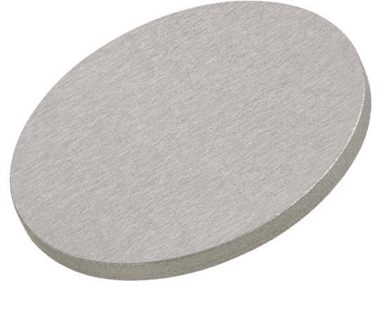
WSi₂ targets are commonly supplied as monolithic discs or plates, and can also be bonded to copper or molybdenum backing plates to enhance heat dissipation and mechanical stability under high-power sputtering conditions. Target dimensions, thickness, and bonding configurations can be customized to suit a wide range of magnetron sputtering systems.
Applications
Tungsten Silicide Sputtering Targets are extensively used in:
Semiconductor integrated circuits (ICs)
Gate electrodes and word lines
Low-resistivity interconnect layers
Diffusion barriers and contact layers
MEMS devices and microfabrication
Advanced research on silicide thin films
Technical Parameters
| Parameter | Typical Value / Range | Importance |
|---|---|---|
| Chemical Formula | WSi₂ | Defines silicide film composition |
| Purity | 99.9% – 99.99% | Ensures electrical and structural consistency |
| Atomic Ratio | W : Si ≈ 1 : 2 | Controls film resistivity and phase stability |
| Diameter | 25 – 300 mm (custom) | Compatible with standard sputtering cathodes |
| Thickness | 3 – 6 mm (typical) | Influences sputtering lifetime |
| Density | ≥ 98% of theoretical | Supports uniform sputtering behavior |
| Backing Plate | Cu / Mo (optional) | Improves thermal management |
Comparison with Related Materials
| Material | Key Advantage | Typical Application |
|---|---|---|
| Tungsten Silicide (WSi₂) | Low resistivity, high thermal stability | Semiconductor gate & interconnects |
| Tungsten (W) | Extremely high melting point | Barrier and contact layers |
| Titanium Silicide (TiSi₂) | Very low resistivity | CMOS interconnects |
FAQ
| Question | Answer |
|---|---|
| Why choose WSi₂ instead of pure tungsten? | WSi₂ offers lower resistivity and better compatibility with silicon devices. |
| Is RF or DC sputtering used for WSi₂? | Both RF and DC sputtering are possible, depending on system design. |
| Can WSi₂ targets be bonded? | Yes, copper or molybdenum backing plates are available. |
| Are custom compositions available? | Custom silicide ratios can be discussed for specific applications. |
| How are the targets packaged? | Vacuum-sealed with moisture and impact protection. |
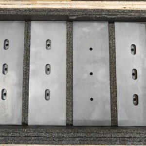
Packaging
Our Tungsten Silicide Sputtering Targets are meticulously cleaned, vacuum-sealed, and packed with reinforced protective materials to prevent contamination and mechanical damage. Clear labeling ensures full traceability throughout storage and transportation.
Conclusion
Tungsten Silicide Sputtering Target (WSi₂) provides a reliable and high-performance solution for depositing low-resistivity, thermally stable silicide thin films. With high purity, excellent compositional control, and customizable dimensions and bonding options, WSi₂ targets are an ideal choice for semiconductor manufacturing and advanced thin film research.
For detailed specifications and a quotation, please contact us at sales@thinfilmmaterials.com.


Reviews
There are no reviews yet.