 MSDS File
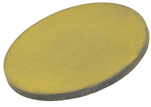
Vanadium Carbide Sputtering Target Description
Vanadium Carbide sputtering target from TFM is a high-quality carbide ceramic material with the chemical formula VC. This target is commonly used in various thin film deposition processes, offering excellent hardness and wear resistance properties, making it ideal for applications in the semiconductor, display, LED, and photovoltaic industries.
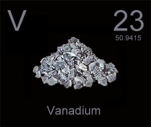
Vanadium is a chemical element with the symbol “V,” named after Vanadis, an old Norse name for the goddess Freyja. It was first identified in 1801 by the scientist M. del Río and later isolated by N.G. Sefström. Vanadium’s atomic number is 23, and it is positioned in Period 4, Group 5 of the periodic table, belonging to the d-block. The relative atomic mass of vanadium is 50.9415(1) Dalton, with the number in brackets indicating the uncertainty of the measurement.
Related Product: Vanadium Sputtering Target
 Carbon is a chemical element with the symbol “C,” originating from the Latin word ‘carbo,’ meaning charcoal. It has been known and used since approximately 3750 BC, with early uses by Egyptians and Sumerians. Carbon holds the atomic number 6 in the periodic table, located at Period 2 and Group 14 within the p-block. The relative atomic mass of carbon is 12.0107(8) Dalton, with the number in brackets indicating the uncertainty of the measurement.
Vanadium Carbide Sputtering Target Handling Notes
1. Indium bonding is recommended for vanadium carbide sputtering targets due to their inherent brittleness and low thermal conductivity, which are characteristics that can pose challenges during the sputtering process.
2. This material’s low thermal conductivity makes it susceptible to thermal shock, necessitating careful handling and appropriate bonding techniques to ensure stable and effective sputtering performance.
Vanadium Carbide Sputtering Target Packaging
Our Vanadium Carbide Sputtering Targets are meticulously tagged and labeled externally to ensure easy identification and stringent quality control. We take great care in handling and packaging these targets to prevent any potential damage during storage or transportation, ensuring the products arrive in pristine condition.
Get Contact
TFM offers Vanadium Carbide Sputtering Targets in various forms, purities, sizes, and prices. We specialize in high-purity thin film deposition materials with optimal density and minimal grain sizes, which are ideal for semiconductor, CVD, and PVD applications in display and optics. Contact Us for current pricing on sputtering targets and other deposition materials that are not listed.

Reviews
There are no reviews yet.