Zinc Antimonide Sputtering Target Description
Zinc Antimonide Sputtering Targets from TFM are renowned for their high quality and exceptional purity. Ideal for thin film deposition techniques like Physical Vapor Deposition (PVD) and Magnetron Sputtering, these targets ensure the production of films with outstanding properties. Due to its excellent electrical conductivity, Zinc Antimonide is extensively used in electronic devices. Moreover, Zinc Antimonide thin-film thermoelectric materials are valued for their safety, non-toxicity, simple structure, abundant raw material availability, and excellent thermal stability. As a result, they are recognized as promising thermoelectric materials with significant application potential.
Related Product: Zinc Sputtering Target, Tin Zinc Sputtering Target
Zinc Antimonide Sputtering Target Specifications
| Compound Formula | ZnSb |
| Molecular Weight | 187.17 |
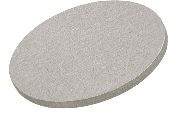
| Appearance | Silver Grey Target |
| Melting Point | – |
| Density | 6.33 g/cm3 |
| Available Sizes | Dia.: 1.0″, 2.0″, 3.0″, 4.0″, 5.0″, 6.0″ Thick: 0.125″, 0.250″ |
Zinc Antimonide Sputtering Target Handling Notes
Indium bonding is advised for Zinc Antimonide Sputtering Targets due to the material’s characteristics that can complicate the sputtering process, such as brittleness and low thermal conductivity. Zinc Antimonide has low thermal conductivity and is prone to thermal shock, making indium bonding a suitable choice to mitigate these issues and ensure reliable performance during the sputtering process.
Zinc Antimonide Sputtering Target Application
Zinc Antimonide thin films, derived from Zinc Antimonide Sputtering Targets, are increasingly significant in the field of thermoelectrics due to their exceptional ability to convert thermal energy into electrical energy. As environmentally friendly materials, Zinc Antimonide offers a direct approach to harnessing and transforming heat into electricity. This capability supports a variety of applications, such as:
- Thermoelectric Power Generation: Efficiently converting heat from industrial processes or waste heat into electrical power.
- Semiconductor Refrigeration: Providing cooling solutions in electronic devices through the thermoelectric effect.
- Sensor Technology: Enhancing the performance of sensors by converting temperature variations into electrical signals.
Zinc Antimonide’s thermoelectric properties contribute to increased sustainability and energy efficiency, making it a valuable material in advanced technology and green energy solutions.
Zinc Antimonide Sputtering Target Packaging
Our Zinc Antimonide Sputtering Target is meticulously handled during storage and transportation to ensure that the quality of the product is maintained in its original condition.


Reviews
There are no reviews yet.