Zinc Oxide doped with Magnesium Sputtering Target Description
Zinc Oxide doped with Magnesium Sputtering Targets offer excellent transparency across both visible and UV spectral ranges, making them ideal for creating optical coatings and transparent conductive films. Their semiconducting properties, derived from both zinc oxide and magnesium oxide, make these targets crucial for manufacturing electronic devices like thin-film transistors and light-emitting diodes. The ratio of zinc oxide to magnesium oxide can be adjusted to modify the bandgap of ZnMgO, providing flexibility in energy band engineering and optoelectronic applications. ZnMgO is also known for its good electrical conductivity, making it suitable for conductive coatings and transparent conductive films. Additionally, ZnMgO demonstrates strong thermal stability at high temperatures, which is beneficial for high-temperature coatings and electronics.
Related Product: Zinc Sputtering Target, Indium Zinc Oxide Sputtering Target
Zinc Oxide doped with Magnesium Sputtering Target Specifications
| Compound Formula | ZnMgO |
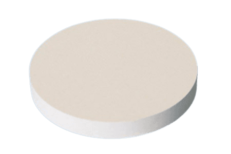
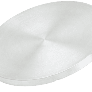
| Appearance | White Target |
| Available Sizes | Dia.: 1.0″, 2.0″, 3.0″, 4.0″, 5.0″, 6.0″ Thick: 0.125″, 0.250″ |
Zinc Oxide doped with Magnesium Sputtering Target Handling Notes
Indium bonding is recommended for Zinc Oxide doped with Magnesium Sputtering Targets because of their inherent brittleness and low thermal conductivity, which can make them challenging for conventional sputtering methods. The material’s low thermal conductivity and susceptibility to thermal shock further underscore the need for indium bonding to enhance its performance and reliability.
Zinc Oxide doped with Magnesium Sputtering Target Application
Zinc Oxide doped with Magnesium Sputtering Target Packaging
Get Contact
TFM offers Zinc Oxide doped with Magnesium Sputtering Targets in a variety of forms, purities, and sizes. We specialize in high-purity physical vapor deposition (PVD) materials, ensuring exceptional density and minimal average grain sizes. These targets are designed for use in semiconductor applications, as well as in chemical vapor deposition (CVD) and physical vapor deposition (PVD) for display and optical technologies.


Reviews
There are no reviews yet.