Introduction
Zinc Oxide (ZnO) Single Crystal Substrate is a wide bandgap semiconductor substrate widely used for epitaxial growth of optoelectronic, piezoelectric, and transparent electronic thin films. With its direct bandgap (~3.37 eV) and high exciton binding energy (~60 meV), ZnO provides an excellent platform for ultraviolet (UV) optoelectronics, transparent conductive devices, and high-frequency acoustic applications.
Due to its wurtzite crystal structure and strong piezoelectric properties, ZnO substrates are also highly attractive for surface acoustic wave (SAW) devices and MEMS applications.
Detailed Description
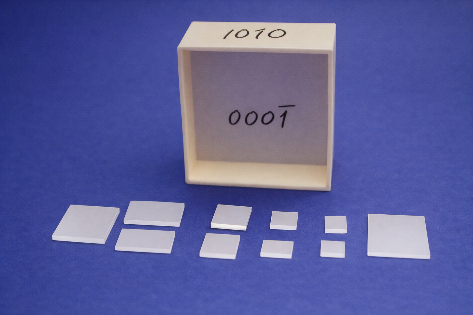
ZnO crystallizes in a hexagonal wurtzite structure, offering polar and non-polar surface orientations that strongly influence thin film growth behavior. The most commonly used orientation is the c-plane (0001), though a-plane and m-plane cuts are also available for specialized research.
Key material characteristics include:
Direct wide bandgap (~3.37 eV at room temperature)
High exciton binding energy (~60 meV)
Strong piezoelectric and pyroelectric properties
High optical transparency in the visible range
Good lattice compatibility with ZnO-based epitaxial layers
ZnO Single Crystal Substrates are grown using hydrothermal or melt-based crystal growth techniques to achieve high crystalline quality and low defect density. After slicing, substrates are precision polished to obtain epi-ready surfaces with low roughness suitable for MBE, MOCVD, sputtering, and PLD deposition.
Depending on application requirements, substrates may be supplied as undoped, n-type doped (e.g., Al-doped), or semi-insulating variants.
Applications
Zinc Oxide (ZnO) Substrates are widely used in:
UV LEDs and laser diodes
Transparent conductive thin films
Surface acoustic wave (SAW) devices
Piezoelectric MEMS devices
Gas and chemical sensors
Transparent thin film transistors (TFTs)
Photodetectors
Optoelectronic research
In ZnO homoepitaxy, lattice matching enables reduced defect density and improved device performance compared with heteroepitaxial growth on sapphire.
Technical Parameters
| Parameter | Typical Value / Range | Importance |
|---|---|---|
| Chemical Formula | ZnO | Wide bandgap semiconductor |
| Crystal Structure | Hexagonal Wurtzite | Determines anisotropic properties |
| Orientation | (0001), (10-10), (11-20) | Influences film growth mode |
| Bandgap | ~3.37 eV | UV optoelectronic performance |
| Surface Finish | SSP / DSP (Epi-ready optional) | Thin film quality |
| Surface Roughness | < 0.5 nm (epi-ready) | Uniform epitaxy |
| Size | 5×5 mm – 20×20 mm (custom) | Deposition compatibility |
| Thickness | 0.3 mm – 1.0 mm | Mechanical stability |
Comparison with Related Materials
| Material | Key Advantage | Typical Application |
|---|---|---|
| ZnO | Direct bandgap + strong piezoelectricity | UV optoelectronics & SAW |
| Sapphire (Al₂O₃) | High thermal stability | ZnO heteroepitaxy |
| GaN | Wide bandgap semiconductor | LEDs & power devices |
| Si | Mature semiconductor platform | Electronics integration |
Compared with sapphire, ZnO substrates provide better lattice matching for ZnO-based thin films, reducing dislocation density. Compared with GaN, ZnO offers stronger excitonic effects and excellent transparency.
FAQ
| Question | Answer |
|---|---|
| What orientations are available? | Common orientations include c-plane (0001), a-plane, and m-plane. |
| Is ZnO suitable for UV devices? | Yes, its wide bandgap and high exciton binding energy make it ideal for UV optoelectronics. |
| Can doped substrates be supplied? | Yes, n-type doped or semi-insulating variants are available upon request. |
| Is the surface epi-ready? | Yes, precision polishing ensures low roughness suitable for epitaxial growth. |
| How is it packaged? | Each substrate is individually packaged in clean, protective containers to prevent contamination and mechanical damage. |
Packaging
Our Zinc Oxide (ZnO) Single Crystal Substrates are meticulously tagged and labeled externally to ensure efficient identification and maintain high standards of quality control. Special care is taken to protect the polished surfaces during storage and transportation, ensuring optimal condition upon arrival.
Conclusion
Zinc Oxide (ZnO) Single Crystal Substrate provides a high-quality wide bandgap semiconductor platform for UV optoelectronics, piezoelectric devices, and transparent electronic applications. With multiple orientation options, excellent crystalline quality, and epi-ready surface preparation, ZnO substrates support advanced research and device development.
For detailed specifications and a quotation, please contact us at sales@thinfilmmaterials.com.


Reviews
There are no reviews yet.