1. Introduction
Microelectronics has revolutionized modern society, powering everything from smartphones and satellites to medical devices and artificial intelligence (AI) systems. In a world increasingly driven by data, traditional computing architectures—based on the von Neumann model—are reaching bottlenecks in energy efficiency, speed, and scalability. Inspired by the human brain, neuromorphic and brain-inspired computing paradigms seek to transcend these limitations, leveraging new architectures and materials for more efficient, adaptive, and intelligent machines.
At the heart of this technological transformation are thin film materials—engineered layers of metals, oxides, semiconductors, and compounds with nanometer-scale thickness. These materials, deposited with atomic precision, are fundamental to the fabrication of advanced devices that emulate synaptic and neuronal functions of biological brains. This article provides a comprehensive exploration of thin film materials for neuromorphic and brain-inspired computing, focusing on their types, deposition techniques, properties, device architectures, challenges, and the critical role of global suppliers like Thin Film Materials (TFM).
2. The Promise of Neuromorphic and Brain-Inspired Computing
2.1. The Von Neumann Bottleneck
Conventional digital computers segregate memory (storage) and processing (logic), resulting in frequent data transfers and significant energy consumption. This so-called von Neumann bottleneck leads to inefficiencies, particularly in AI and machine learning tasks that require massive parallelism and real-time data processing.
2.2. Brain-Inspired Architectures
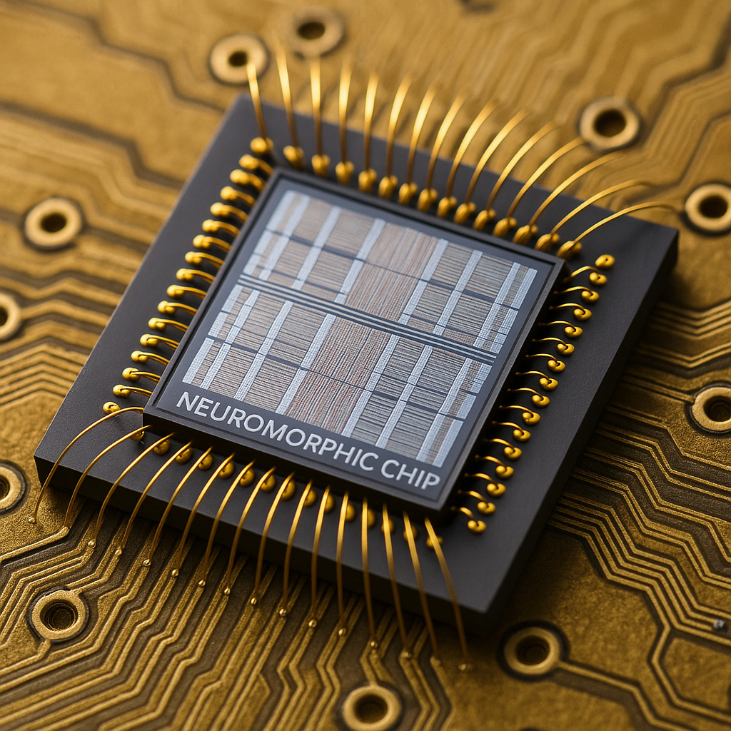
Neuromorphic computing architectures mimic the structure and function of biological neural networks. They integrate memory and processing in the same physical location—analogous to synapses in the brain—enabling parallelism, adaptability, and ultra-low power consumption.
2.3. Key Requirements for Hardware
To realize neuromorphic computing, hardware platforms must support:
- Non-volatile, analog memory states (like biological synapses)
- High-density integration and scalability
- Energy-efficient operation
- Biocompatibility (for biohybrid applications)
- Reconfigurability and reliability
Thin film materials are uniquely positioned to meet these requirements thanks to their tunable properties, compatibility with modern microfabrication, and adaptability to diverse device architectures.
3. Thin Film Materials: An Overview
3.1. Definition and Relevance
Thin film materials are layers—ranging from a few nanometers to several microns in thickness—deposited on substrates via physical or chemical processes. Their electronic, magnetic, optical, and ionic properties can be engineered through composition, structure, and processing conditions.
3.2. Types of Thin Film Materials in Neuromorphic Devices
- Metals (e.g., Pt, TiN, Au): Electrodes and interconnects
- Oxides (e.g., HfO2, Ta2O5, SrTiO3, TiO2): Resistive switching, ferroelectric, and memristive layers
- Chalcogenides (e.g., Ge2Sb2Te5): Phase-change memory
- Organic materials and polymers: Flexible and biocompatible devices
- 2D materials (e.g., MoS2, graphene): Atomically thin, tunable properties
- Complex oxides (e.g., perovskites): Multifunctional, emergent phenomena
The selection of material is dictated by the desired device function, compatibility with processing, and required performance metrics.
4. Thin Film Deposition Techniques for Neuromorphic Devices
4.1. Physical Vapor Deposition (PVD)
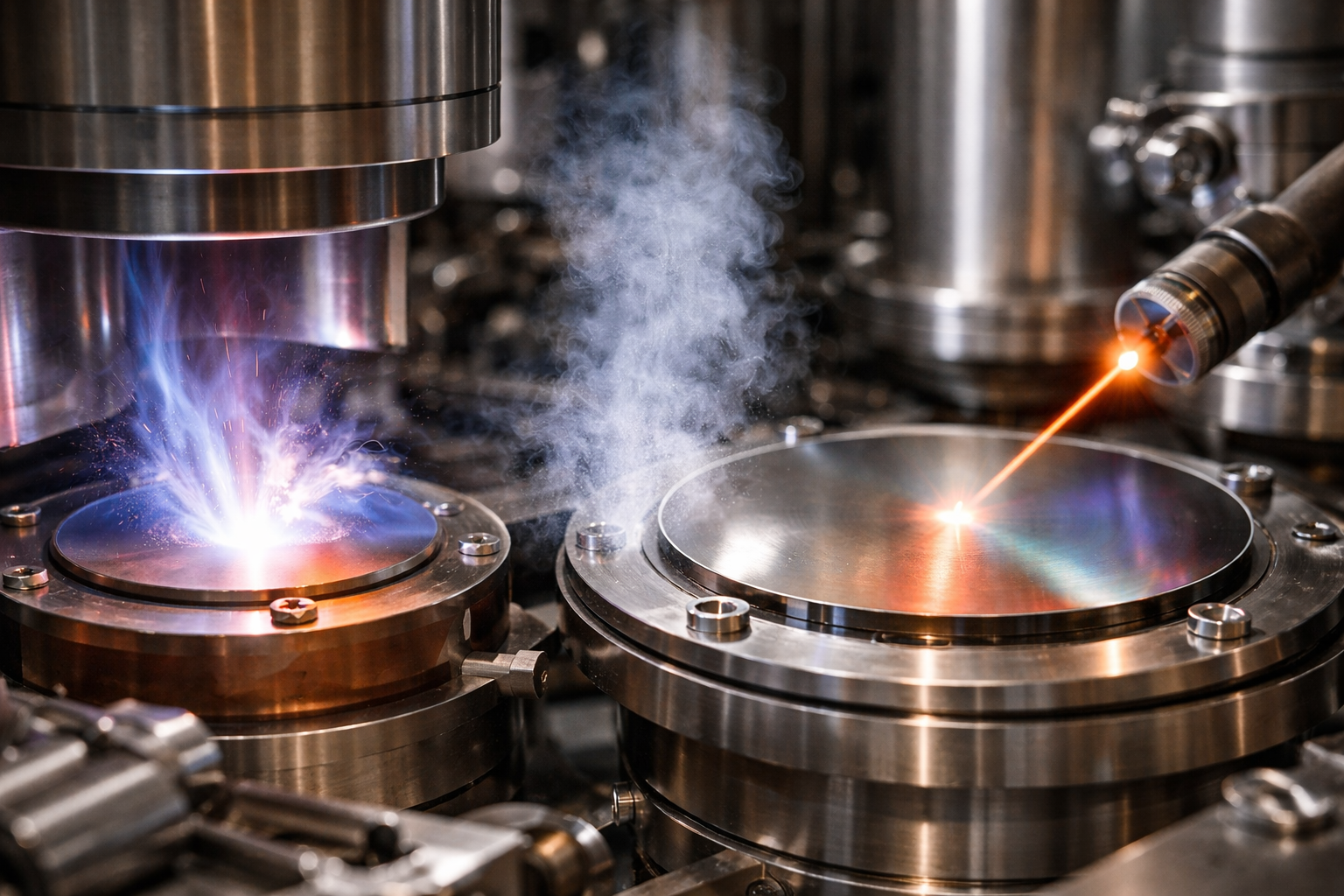
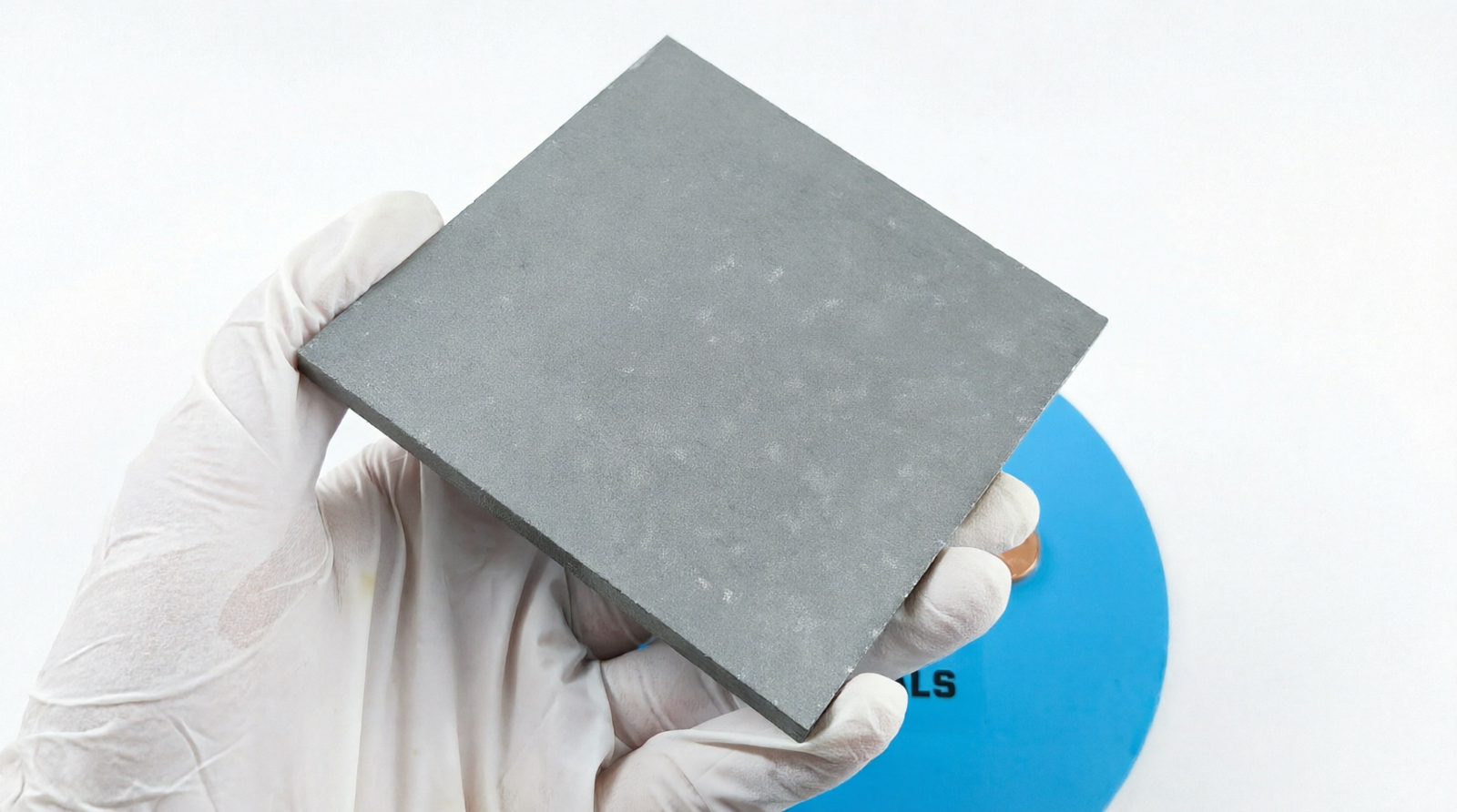
Sputtering: Magnetron sputtering is widely used for depositing metals, alloys, oxides, and ceramic thin films with excellent control over thickness and composition. Sputtering targets from suppliers like TFM enable deposition of high-purity conductive and resistive layers.
Thermal and Electron-Beam Evaporation: Used for metals, chalcogenides, and some oxides. Micro-electronic evaporation sources allow precise, uniform films, essential for device miniaturization and high integration.
4.2. Chemical Vapor Deposition (CVD)
CVD processes are used to grow high-quality thin films of semiconductors (e.g., Si, Ge), transition metal dichalcogenides (e.g., MoS2), and dielectrics on various substrates. Atomic layer deposition (ALD) offers sub-nanometer control, crucial for scaling down device dimensions and ensuring uniformity.
4.3. Solution-Based Methods
Spin coating, inkjet printing, and sol-gel processes are employed for organic, polymer, and some oxide thin films. These methods are compatible with flexible substrates and large-area deposition.
4.4. Epitaxial Growth
For complex oxides and heterostructures, techniques like pulsed laser deposition (PLD) and molecular beam epitaxy (MBE) allow atomic-level control, enabling the creation of high-quality interfaces and engineered functionalities.
5. Key Thin Film Materials for Neuromorphic Computing
5.1. Metal Oxides
- Hafnium Oxide (HfO2): Used in resistive random-access memory (ReRAM) and memristors. HfO2 thin films exhibit stable resistive switching, scalability, and compatibility with CMOS processes.
- Titanium Oxide (TiO2): Demonstrates resistive switching and has been extensively studied for neuromorphic synapses. TiO2 films are also corrosion-resistant and used as electrodes in bioelectronic applications.
- Tantalum Oxide (Ta2O5): Shows robust switching characteristics, high endurance, and retention, making it ideal for non-volatile memory devices.
- Strontium Titanate (SrTiO3): A perovskite oxide with tunable properties, suitable for ferroelectric and memristive devices.
- Nickel Oxide (NiO): P-type oxide with resistive switching and synaptic plasticity behaviors.
5.2. Chalcogenides
- Ge2Sb2Te5 (GST): The archetypal phase-change material, GST enables fast, reversible switching between amorphous and crystalline states. Used in phase-change memory (PCM) devices that mimic synaptic weight changes.
5.3. Ferroelectric Materials
Ferroelectric thin films, such as Pb(Zr,Ti)O3 (PZT) and HfO2-based ferroelectrics, offer non-volatile, analog memory states. Their spontaneous polarization can be tuned with an electric field, enabling synaptic-like behavior.
5.4. Transition Metal Dichalcogenides (TMDs) and 2D Materials
Materials like MoS2, WS2, and graphene are atomically thin, allowing for flexible, transparent, and highly scalable neuromorphic devices. Their electrostatic and optical properties are tunable via thickness and stacking.
5.5. Organic and Polymer Materials
Polymers and organic molecules bring flexibility, biocompatibility, and low-cost processing. They are used in artificial synapses and neuromorphic devices, especially for soft, wearable, or implantable applications.
5.6. Complex Oxides and Perovskites
Perovskite oxides (e.g., SrTiO3, LaAlO3, BaTiO3) display a wide range of functionalities—ferroelectricity, magnetoresistance, and superconductivity—arising from their lattice structures and electronic correlations.
5.7. High-Purity Metals and Alloys
Thin films of metals such as platinum (Pt), gold (Au), titanium nitride (TiN), and alloys serve as electrodes, interconnects, and diffusion barriers. For neuromorphic devices operating in biological environments, corrosion-resistant and biocompatible metals are essential.
6. Functional Properties Required for Neuromorphic Thin Films
6.1. Electrical Properties
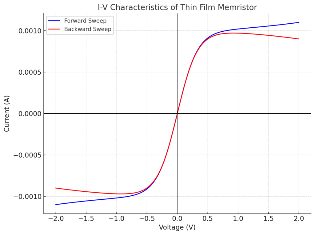
- Resistive switching (memristive behavior): Enables non-volatile, analog memory for synaptic emulation.
- High/low resistance ratios: Distinguishes between memory states.
- Low leakage currents: Reduces power consumption.
- Stable endurance and retention: Ensures reliable operation and long device lifetimes.
6.2. Ionic and Electronic Transport
Materials must support controlled movement of ions (e.g., oxygen vacancies in oxides, metal cations in ECM devices) or electrons to modulate conductivity and emulate synaptic plasticity.
6.3. Ferroelectric and Piezoelectric Properties
Ferroelectric thin films exhibit switchable polarization, enabling analog memory states and non-destructive readout. Piezoelectricity allows for sensing and actuation in bio-interfaced neuromorphic systems.
6.4. Structural and Interfacial Quality
Uniform, defect-free thin films are crucial for device reproducibility, scalability, and endurance. High-quality interfaces minimize unwanted reactions and enhance device performance.
6.5. Biocompatibility and Flexibility
For biohybrid and implantable neuromorphic devices, thin films must be non-toxic, stable in physiological environments, and mechanically flexible.
7. Device Architectures Enabled by Thin Films
7.1. Memristors and Resistive Switching Memories (ReRAM)
Memristors are two-terminal devices whose resistance depends on the history of applied voltage/current—mimicking synaptic plasticity. They consist of a thin film of switching material (e.g., HfO2, TiO2, Ta2O5) sandwiched between two electrodes. The movement of ions or defects under an electric field modulates the film’s resistance.
7.2. Phase-Change Memory (PCM) Devices
PCM devices exploit the reversible transition between amorphous and crystalline phases in chalcogenide thin films (e.g., GST). The two phases have distinct electrical conductivities, representing different memory states.
7.3. Ferroelectric Memories and Synaptic Devices
Ferroelectric thin films (e.g., HfO2) allow for the storage of analog states via polarization switching. These devices offer low-voltage operation, multi-level memory, and compatibility with CMOS processes.
7.4. Electrochemical Metallization (ECM) Cells
Also known as conductive-bridge RAM (CBRAM), these devices use thin films of solid electrolytes (e.g., Ag-doped SiO2) to form and dissolve metallic filaments, enabling non-volatile switching.
7.5. Organic and Polymer Artificial Synapses
Organic thin films enable low-power, flexible, and biocompatible neuromorphic devices. Their properties can be engineered via molecular design and blending.
7.6. Hybrid and Heterostructure Architectures
Combining multiple thin film materials—such as 2D materials with oxides—can introduce new functionalities, interface effects, and enhanced device performance.
8. Case Studies: Material Systems in Neuromorphic Prototypes
8.1. HfO2-Based Memristors
Hafnium oxide thin films, deposited by magnetron sputtering or ALD, are a leading platform for memristive devices. They offer:
- High scalability, with sub-10 nm films
- Endurance (>109 cycles) and retention (years at room temperature)
- Compatibility with silicon technology for large-scale integration
HfO2-based memristors have demonstrated unsupervised learning, spike-timing-dependent plasticity (STDP), and pattern recognition in hardware.
8.2. TiO2 Artificial Synapses
TiO2 thin films exhibit resistive switching due to the migration of oxygen vacancies. Devices have shown:
- Gradual, analog conductance modulation (synaptic weight update)
- Low switching voltages and high endurance
- Integration into crossbar arrays for high-density memory
Their chemical stability makes TiO2 films suitable for implantable biohybrid devices.
8.3. GST Phase-Change Memories
Phase-change memory cells using GST thin films offer:
- Fast switching (<100 ns) between high and low resistance states
- Multi-level storage (analog states for synaptic emulation)
- Scalability down to sub-20 nm dimensions
PCM devices are being explored for on-chip learning and hardware neural networks.
8.4. 2D Materials-Based Neuromorphic Devices
MoS2 and other TMD thin films, grown by CVD or exfoliation, have enabled:
- Ultra-thin, flexible synaptic devices
- Gate-tunable conductance for analog memory
- Integration with optoelectronic functions (e.g., artificial retina)
8.5. Organic and Polymer Synaptic Transistors
Organic thin-film transistors (OTFTs) based on polymers like PEDOT:PSS demonstrate:
- Biocompatibility and mechanical flexibility
- Low-power operation (<1 V)
- Application in artificial skin and wearable sensors
8.6. Perovskite and Complex Oxide Heterostructures
Thin films of perovskite oxides, grown by PLD or MBE, enable devices with:
- Multifunctional properties (ferroelectricity, magnetism, superconductivity)
- Emergent phenomena at interfaces (e.g., 2DEG formation)
- Potential for adaptive, reconfigurable neuromorphic systems
9. Role of Thin Film Materials Suppliers
9.1. Material Diversity and Quality
The success of neuromorphic hardware depends critically on the availability of high-purity, precisely engineered thin film materials. Suppliers like Thin Film Materials (TFM) provide:
- A portfolio of over 3,000 advanced materials, covering metals, alloys, oxides, ceramics, and rare-earth compounds
- Custom sputtering targets and evaporation sources tailored for specific device applications
- Vacuum coating materials for high-uniformity, defect-free films
- High-purity metals and compounds for critical device layers (e.g., electrodes, diffusion barriers)
9.2. Support for Research and Manufacturing
TFM and similar suppliers support both R&D and large-scale production by:
- Providing small quantities for prototyping and iterative device optimization
- Offering bulk quantities for industrial fabrication
- Ensuring material traceability and quality control
- Assisting with deposition process optimization and troubleshooting
9.3. Integration with Advanced Deposition Technologies
Suppliers enable integration of thin film materials into advanced deposition platforms, such as:
- Magnetron sputtering systems for uniform oxide and nitride films
- Thermal and e-beam evaporation for high-purity metals and chalcogenides
- ALD and CVD for atomically controlled films
The availability of custom-shaped targets, high-purity crucibles, and precision evaporation sources is essential for reliable and reproducible thin film deposition.
10. Challenges and Future Perspectives
10.1. Material and Device Scalability
As neuromorphic hardware moves towards large-scale deployment, challenges include:
- Downscaling device dimensions while maintaining performance and reliability
- Uniform deposition of thin films over large wafer areas
- Defect control and interface engineering
10.2. Variability and Reproducibility
Thin film devices, especially those relying on defect dynamics (e.g., memristors), can exhibit device-to-device and cycle-to-cycle variability. Addressing this requires:
- Improved control over film stoichiometry and microstructure
- Advanced metrology and characterization
- Material engineering to tune defect densities and distributions
10.3. Integration with CMOS and Heterogeneous Architectures
Ensuring compatibility with existing semiconductor manufacturing processes is crucial for commercialization. This includes:
- Low-temperature deposition processes
- Etch selectivity and patterning of thin films
- Hybrid integration with logic, memory, and sensing components
10.4. New Materials Discovery and Design
Ongoing research seeks new thin film materials with improved properties:
- Materials with intrinsic neuromorphic functionalities (e.g., plasticity, learning rules)
- Bio-inspired materials for interface with living tissue
- Environmentally sustainable and abundant materials
High-throughput computation and AI-assisted materials discovery are accelerating this search.
10.5. Reliability, Endurance, and Aging
For real-world deployment, neuromorphic devices must demonstrate:
- Long-term operational stability under electrical and environmental stress
- Resistance to fatigue, corrosion, and electromigration
- Predictable aging and failure modes
Suppliers play a key role by providing materials with certified purity and stability.
10.6. Standardization and Benchmarking
The field requires standardized protocols for material performance, device benchmarking, and reliability testing to enable cross-comparison and accelerate commercialization.
11. Conclusion
Thin film materials are foundational to the ongoing revolution in neuromorphic and brain-inspired computing. Their tunable properties, compatibility with advanced microfabrication, and adaptability to diverse device architectures make them indispensable for emulating the complex functions of biological neural systems. As the field transitions from laboratory prototypes to large-scale, real-world applications, the role of high-quality material suppliers like Thin Film Materials (TFM) becomes increasingly critical.
Delivering over 3,000 advanced materials—including metals, oxides, ceramics, and rare-earth compounds—TFM supports both research and industrial-scale manufacturing of next-generation neuromorphic hardware. Their expertise in customized sputtering targets, evaporation sources, and process optimization ensures that device innovators have access to the materials they need, when they need them, with the highest standards of quality and service.
As neuromorphic computing paves the way for ultra-efficient AI, adaptive edge devices, and brain-machine interfaces, continued advances in thin film materials—driven by close collaboration between researchers, manufacturers, and suppliers—will remain at the forefront of the field. The journey towards brain-like computing is, in many ways, a journey through the science and engineering of thin films.
References and Further Reading
- Wong, H.-S. P., & Salahuddin, S. (2015). Memory leads the way to better computing. Nature Nanotechnology, 10(3), 191–194.
- Yang, J. J., Strukov, D. B., & Stewart, D. R. (2013). Memristive devices for computing. Nature Nanotechnology, 8(1), 13–24.
- Ielmini, D., & Wong, H.-S. P. (2018). In-memory computing with resistive switching devices. Nature Electronics, 1(6), 333–343.
- Thin Film Materials (TFM) Product Catalog and Technical Resources
Related Products
Hafnium Oxide (HfO₂) Sputtering Target

