1. Introduction: Quantum Materials Meet Thin-Film Technology
Quantum materials—systems whose macroscopic properties arise from quantum mechanical phenomena such as electron correlation, topology, and spin entanglement—represent one of the most dynamic frontiers in condensed matter physics. Over the past decade, the marriage between quantum materials and thin-film engineering has transitioned from a laboratory curiosity to a viable platform for quantum devices, superconducting circuits, and spintronic technologies.
While bulk crystals have traditionally been the foundation for studying quantum phenomena, thin films provide unprecedented control over structural order, strain, composition, and interfaces. This tunability allows researchers to stabilize metastable phases, enhance quantum coherence, and integrate quantum materials into scalable device architectures.
Recent studies from institutions such as MIT’s Quantum Engineering Group and Lawrence Berkeley National Laboratory have demonstrated how epitaxial thin films of correlated oxides and topological insulators can host emergent electronic phases that are not accessible in their bulk forms. Similarly, resources like the Materials Project Database and Nature Materials provide extensive datasets and peer-reviewed research enabling the design and prediction of thin-film-based quantum heterostructures.
In this article, we explore the current status and emerging directions of thin films as practical quantum materials—highlighting fabrication approaches, interfacial phenomena, measurement techniques, and potential applications that could shape the future of quantum electronics. For readers interested in applied perspectives, organizations such as Center for Quantum Materials (University of Maryland) and European Quantum Technology Flagship provide excellent overviews of global efforts in thin-film quantum integration.
2. Defining Quantum Materials
Quantum materials encompass a diverse class of compounds exhibiting collective quantum effects that defy classical descriptions. Common categories include:
| Type | Representative Materials | Key Quantum Phenomenon |
|---|---|---|
| Topological Insulators | Bi₂Se₃, Sb₂Te₃ | Surface states protected by topology |
| 2D Quantum Systems | Graphene, MoS₂ | Quantum Hall effect, valleytronics |
| Strongly Correlated Oxides | VO₂, SrTiO₃, LaNiO₃ | Mott transitions, charge ordering |
| Superconductors | NbN, YBCO, FeSe | Cooper pairing, quantum coherence |
| Magnetic Quantum Materials | CrI₃, MnBi₂Te₄ | Spin frustration, spin–orbit coupling |
| Topological Superconductors | FeTe₁₋ₓSeₓ, Bi/Nb hybrids | Majorana zero modes |
These materials often exhibit phase competition and emergent behaviors—making them ideal for exploration in epitaxial thin-film form, where structure, strain, and symmetry can be precisely tuned.
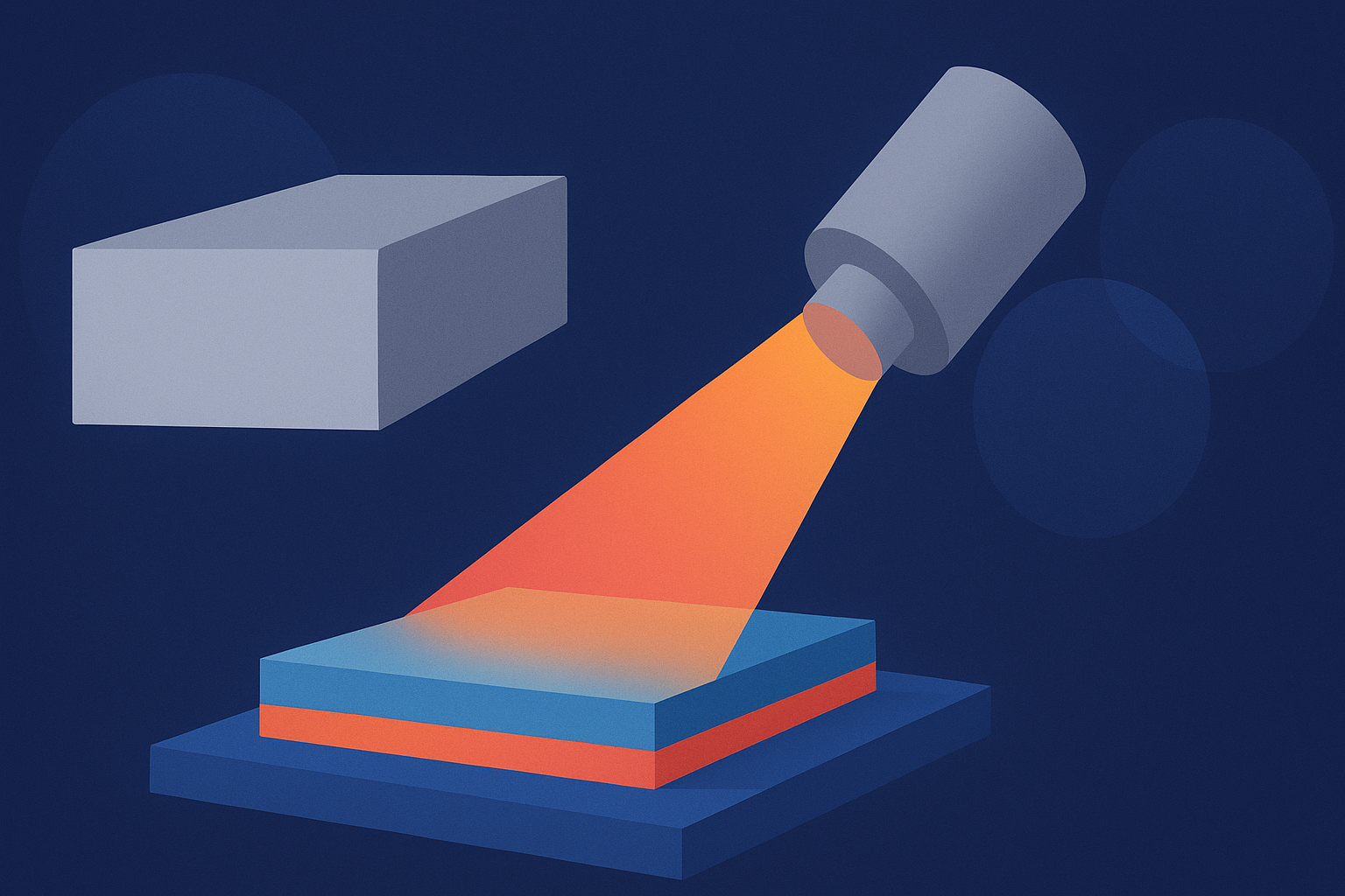
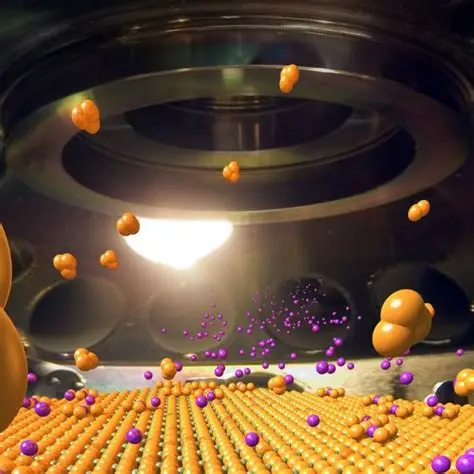
3. Thin-Film Growth: Enabling Quantum Control
3.1 Molecular Beam Epitaxy (MBE)
MBE is the gold standard for atomically precise growth of quantum materials. Ultra-high vacuum environments minimize contamination, while in-situ RHEED monitoring enables monolayer control.
Examples:
- Growth of Bi₂Se₃ and Bi₂Te₃ topological insulators with atomically flat terraces.
- Epitaxial FeSe on SrTiO₃, where interfacial phonon coupling enhances superconducting Tc from 8 K (bulk) to over 65 K.
3.2 Pulsed Laser Deposition (PLD)
PLD is widely used for complex oxides and correlated materials. High-energy laser ablation enables stoichiometric transfer, critical for transition metal oxides such as LaAlO₃/SrTiO₃ (LAO/STO), which exhibits a two-dimensional electron gas (2DEG) at the interface.
3.3 Atomic Layer Deposition (ALD)
ALD provides conformal coating and angstrom-level thickness control—crucial for integrating quantum materials with 3D device architectures and hybrid semiconductor structures.
3.4 Hybrid and Nonequilibrium Routes
Emerging approaches such as hybrid MBE, sputtering-assisted epitaxy, and laser molecular-beam epitaxy enable metastable phase formation (e.g., perovskite nickelates and topological ferromagnets) that are otherwise inaccessible in bulk.
4. Quantum Effects in Thin-Film Systems
4.1 Dimensional Confinement
When film thickness approaches electronic coherence length (~1–10 nm), quantum confinement modifies the electronic band structure—often leading to discrete energy levels and enhanced electron correlations.
4.2 Interface-Driven Phenomena
Interfaces between quantum materials introduce broken symmetry, charge transfer, and orbital reconstruction.
Classic examples:
- LAO/STO interface: Emergence of 2DEG and superconductivity at 10 nm scale.
- FeSe/SrTiO₃ interface: Enhancement of Tc due to cross-interface electron–phonon coupling.
4.3 Strain Engineering
Epitaxial strain in thin films can modify lattice symmetry and bandwidth, thus controlling metal–insulator transitions.
For instance, SrRuO₃ thin films under tensile strain exhibit altered magnetic anisotropy, while VO₂ strain-tuned epitaxy allows phase-change control at lower switching energy.
4.4 Spin–Orbit and Topological Effects
Thin films of heavy-element materials (e.g., Bi, WTe₂, and PtSe₂) exhibit strong spin–orbit coupling (SOC), crucial for topological protection and spin–charge conversion in spintronic devices.
5. Experimental Characterization Techniques
5.1 Structural Probes
- High-Resolution X-ray Diffraction (HRXRD): Determines lattice mismatch, epitaxial orientation, and strain.
- Transmission Electron Microscopy (TEM): Visualizes atomic interfaces and defect structures.
- Scanning Probe Microscopy (SPM): Maps surface morphology and local conductivity.
5.2 Electronic and Quantum Characterization
- Angle-Resolved Photoemission Spectroscopy (ARPES): Directly measures the band dispersion and topological states.
- Scanning Tunneling Microscopy/Spectroscopy (STM/STS): Resolves local density of states and quasiparticle interference.
- Magnetotransport Measurements: Hall and Shubnikov–de Haas oscillations reveal carrier quantization and Berry phase.
5.3 Ultrafast and Optical Techniques
Time-resolved spectroscopy provides insight into nonequilibrium quasiparticle dynamics, enabling the study of coherent phonon–electron coupling in quantum films.
6. Case Studies in Quantum Thin Films
6.1 Topological Insulators: Bi₂Se₃ and Beyond
Thin films of Bi₂Se₃ retain robust surface states even down to ~6 quintuple layers, though hybridization can open small gaps. Interface engineering with magnetic or superconducting layers allows exploration of quantum anomalous Hall effects and Majorana bound states.
6.2 Transition Metal Dichalcogenides (TMDs)
Monolayer MoS₂, WSe₂, and NbSe₂ thin films exhibit direct bandgaps and strong spin–valley coupling, paving the way for valleytronic and quantum light-emitting devices.
6.3 Oxide Interfaces
The LaAlO₃/SrTiO₃ (LAO/STO) interface is an archetype of emergent quantum phenomena:
- Conductivity arises above 4 unit cells of LAO.
- Coexistence of superconductivity and magnetism.
- Tunable 2DEG carrier density via gating.
6.4 Iron-Based Superconductors
Epitaxial thin films of FeSe, FeTe₁₋ₓSeₓ, and BaFe₂As₂ have demonstrated enhanced Tc values due to interfacial strain and electronic reconstruction, making them promising for quantum computing interconnects.
7. Integration with Device Platforms
The transition from research to practical quantum technology requires integration of quantum films with semiconductor, superconducting, and photonic platforms.
| Application | Integration Example | Function |
|---|---|---|
| Quantum Computing | NbN films in Josephson junctions | Qubit superconducting circuits |
| Spintronics | Bi₂Se₃ / CoFeB heterostructures | Spin Hall effect devices |
| Quantum Sensing | Diamond films with NV centers | Atomic-scale magnetometry |
| Photonics | 2D perovskite films | Quantum light emission |
Heterogeneous integration through wafer bonding or hybrid epitaxy enables scalable architectures without compromising quantum coherence.
8. Challenges Toward Practical Implementation
Despite remarkable progress, several bottlenecks limit the commercialization of thin-film quantum materials:
8.1 Material Uniformity and Defects
Defects and dislocations act as quantum decoherence centers, degrading mobility and topological protection. Uniform large-area growth remains challenging, especially for 2D TMDs and oxides.
8.2 Interface Quality
Atomic intermixing or contamination at heterointerfaces can obscure or suppress emergent states. In-situ transfer and surface passivation techniques are essential for maintaining quantum fidelity.
8.3 Scalability and Stability
Maintaining epitaxial precision over wafer-scale substrates without phase segregation or oxidation is a key hurdle for industrial adoption.
8.4 Quantum Device Compatibility
Integrating quantum films with CMOS or cryogenic electronics requires thermal, chemical, and mechanical compatibility, along with standardized processing routes.
9. Future Directions and Opportunities
9.1 Artificial Quantum Heterostructures
Atomic-layer stacking allows “designer quantum materials,” combining topological, magnetic, and superconducting layers to realize exotic quantum phases like axion insulators and Majorana networks.
9.2 Straintronics and Field-Tunable Quantum States
Strain, electric, or optical fields can modulate topological band inversions, enabling nonvolatile control of quantum states in flexible or reconfigurable devices.
9.3 Quantum Neuromorphic Systems
Quantum thin films with tunable resistance or spin textures (e.g., memristive oxide junctions) are potential candidates for brain-inspired computing architectures.
9.4 Sustainable Quantum Material Processing
Low-temperature and solution-based deposition routes (e.g., metal-organic decomposition, ALD) can reduce environmental impact while enabling mass manufacturability.
10. Conclusion
The integration of quantum materials into thin-film platforms is transforming the landscape of condensed matter research and quantum device engineering. Thin films offer atomic-level control, scalability, and tunable quantum interactions—qualities essential for next-generation technologies such as quantum computers, topological sensors, and spin-based electronics.
As synthesis methods mature and interfacial understanding deepens, thin-film quantum materials will likely transition from the research bench to commercial quantum devices—bridging the gap between quantum phenomena and practical engineering.