1. Introduction
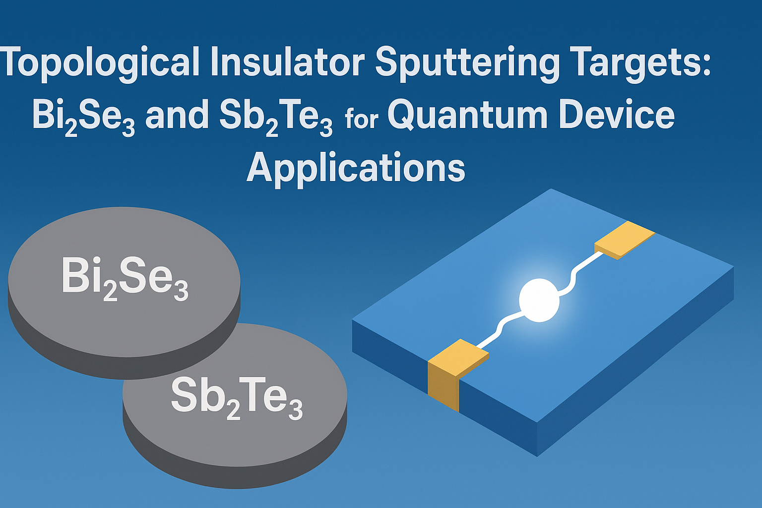
The rapid evolution of quantum technologies and advanced electronics has spurred substantial interest in novel materials with unique electronic properties. Topological insulators (TIs) have emerged as a particularly exciting class of quantum materials, characterized by insulating bulk states and robust, spin-polarized conducting surface states protected by time-reversal symmetry. Among the most studied TIs are bismuth selenide (Bi₂Se₃) and antimony telluride (Sb₂Te₃), which exhibit large bulk band gaps and simple surface state structures, making them ideal candidates for both fundamental research and practical device applications.
Sputtering targets of Bi₂Se₃ and Sb₂Te₃ are pivotal for the fabrication of high-quality thin films vital to quantum device engineering, such as topological transistors, quantum spin Hall devices, and advanced sensors. This article provides an in-depth analysis of Bi₂Se₃ and Sb₂Te₃ sputtering targets, their properties, fabrication techniques, challenges, and their crucial role in quantum device applications.
2. Topological Insulators: An Overview
2.1 Fundamental Properties
Topological insulators are materials that are insulating in their interior but possess metallic, spin-polarized surface states. These surface states are protected by topological invariants arising from the material’s band structure, rendering them robust against non-magnetic impurities and disorder.
2.2 Quantum Device Relevance
The unique surface states of TIs exhibit spin-momentum locking, essential for low-dissipation spintronic devices, quantum computation, and next-generation information storage. Thin films of TIs are particularly attractive for device miniaturization and integration with existing semiconductor technology.
2.3 Why Bi₂Se₃ and Sb₂Te₃?
Bi₂Se₃ and Sb₂Te₃ stand out due to:
– Large bulk band gaps (~0.3 eV for Bi₂Se₃, ~0.28 eV for Sb₂Te₃),
– Simple Dirac cone surface state dispersion,
– Availability of high-purity source materials,
– Compatibility with standard thin-film deposition techniques,
– Well-understood surface chemistry and stability.
3. Sputtering Deposition in Thin Film Fabrication
3.1 Sputtering: The Basics
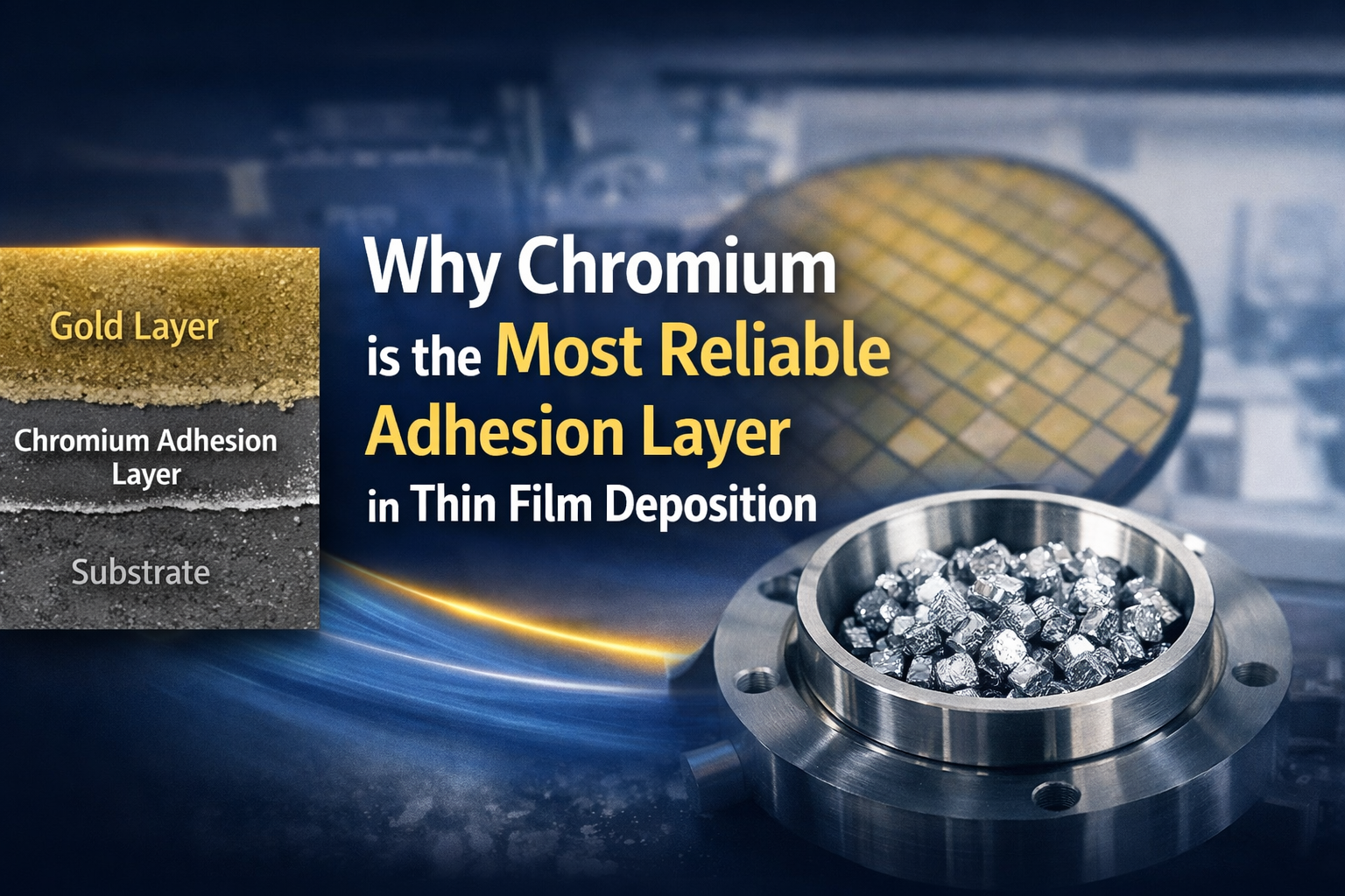
Sputtering is a physical vapor deposition (PVD) technique wherein energetic ions (often Ar⁺) bombard a target, ejecting atoms that then deposit onto a substrate, forming a thin film. The process allows for precise control over film composition, thickness, and uniformity, making it a workhorse for research and industrial applications alike.
3.2 Sputtering Target: Definition and Role
A sputtering target is the source material bombarded in the sputtering process. The quality, purity, and composition of the target directly influence the properties of the resultant thin film. For TIs, maintaining stoichiometry and high purity is paramount to preserve the unique electronic features.
3.3 Types of Sputtering
– **DC Sputtering**: Suitable for conductive targets.
– **RF Sputtering**: Necessary for insulating or semiconducting targets like Bi₂Se₃ and Sb₂Te₃.
– **Magnetron Sputtering**: Enhances plasma density and deposition rates.
4. Bi₂Se₃ Sputtering Targets: Properties and Specifications
4.1 Chemical and Physical Properties
– **Chemical Formula**: Bi₂Se₃
– **Appearance**: Gray solid
– **Density**: 9.20 g/cm³
– **Melting Point**: ~2,000 °C
– **Purity Levels**: 99.9%, 99.95%, 99.99%, 99.995%, 99.999%
– **Available Shapes**: Discs, plates, column targets, step targets, custom shapes
– **Available Sizes**: Diameters from 1.0″ to 6.0″; thicknesses from 0.125″ to 0.250″
4.2 Material Challenges
– **Brittleness**: Bi₂Se₃ is mechanically fragile, complicating handling and mounting.
– **Low Thermal Conductivity**: Prone to thermal gradients and potential cracking during sputtering.
– **Thermal Shock Susceptibility**: Rapid temperature changes can cause mechanical failure.
4.3 Handling and Bonding
Due to brittleness and low thermal conductivity, **indium bonding** is highly recommended for mounting Bi₂Se₃ sputtering targets. This soft metal provides a compliant, thermally conductive interface, alleviating stress and improving thermal management during sputtering.
4.4 Purity and Stoichiometry
Maintaining high purity and precise stoichiometry is critical. Impurities can introduce scattering centers, reducing surface state mobility and degrading device performance. Thin Film Materials (TFM) offers Bi₂Se₃ targets up to 99.999% purity, ensuring minimal contamination.
5. Sb₂Te₃ Sputtering Targets: Properties and Specifications
5.1 Chemical and Physical Properties
– **Chemical Formula**: Sb₂Te₃
– **Appearance**: Gray solid (typically metallic luster)
– **Density**: ~6.50 g/cm³
– **Melting Point**: ~620 °C
– **Purity Levels**: 99.9%, 99.95%, 99.99%, 99.995%, 99.999%
– **Available Shapes**: Discs, plates, columns, step targets, custom shapes
– **Available Sizes**: Diameters from 1.0″ to 6.0″; thicknesses from 0.125″ to 0.250″
5.2 Material Challenges
– **Low Melting Point**: Sb₂Te₃ is more susceptible to melting or deformation under high power sputtering.
– **Brittleness and Volatility**: Like Bi₂Se₃, it is brittle and can lose stoichiometry if not carefully processed.
5.3 Handling and Bonding
Indium or elastomer bonding is common, particularly for larger targets or high-power sputtering, to prevent cracking and ensure uniform cooling.
5.4 Purity and Stoichiometry
High-purity Sb₂Te₃ targets (up to 99.999%) are essential for fabricating films with optimal topological properties and minimal defect density.
6. Fabrication of Sputtering Targets
6.1 Raw Material Synthesis
- Elemental Mixing: High-purity bismuth, selenium / antimony, and tellurium are weighed in precise stoichiometric ratios to ensure the correct chemical composition.
- Melting and Alloying: The elements are melted together in evacuated quartz ampoules, often using a rocking furnace to achieve uniform mixing and homogeneity.
- Solidification: Controlled cooling, sometimes via directional solidification, produces polycrystalline ingots suitable for further processing into sputtering targets.
6.2 Target Shaping and Finishing
– **Cutting and Grinding**: Ingots are sliced to required dimensions and ground for flatness.
– **Polishing**: Surfaces are polished to improve interface bonding and ensure uniform sputtering.
– **Bonding**: Targets are bonded to backing plates (typically copper or stainless steel) using indium or specialized elastomers.
6.3 Quality Control
– **X-ray Diffraction (XRD)**: Confirms phase purity and crystallinity.
– **Inductively Coupled Plasma Mass Spectrometry (ICP-MS)**: Ensures elemental purity.
– **Visual and Mechanical Inspection**: Checks for cracks, voids, or other defects.
7. Sputtering Process Optimization for TI Thin Films
7.1 Process Parameters
– **Working Pressure**: 1–10 mTorr, optimized for film density and uniformity.
– **Substrate Temperature**: 100–400 °C; higher temperatures improve crystallinity but may volatilize elements.
– **Sputter Power**: 10–100 W (RF), with lower powers reducing target overheating.
– **Gas Flow**: High-purity Argon, sometimes with a small addition of chalcogen vapor (Se or Te) to compensate for possible loss.
7.2 Substrate Selection and Preparation
– **Common Substrates**: SiO₂/Si, sapphire (Al₂O₃), SrTiO₃, mica.
– **Preparation**: Ultrasonic cleaning, plasma or ozone treatment to ensure cleanliness and promote adhesion.
7.3 Film Growth and Post-Annealing
– **In-situ Annealing**: May be applied during or after deposition to enhance grain growth and reduce defects.
– **Capping Layers**: Sometimes used to prevent oxidation of TI films.
7.4 Challenges in TI Thin Film Growth
– **Stoichiometry Control**: Se or Te can be lost due to volatility, requiring careful tuning of process parameters.
– **Film Uniformity**: Target composition, plasma density, and substrate rotation impact thickness and compositional uniformity.
– **Defect Minimization**: Grain boundaries and dislocations can scatter carriers and degrade surface state properties.
8. Applications of Bi₂Se₃ and Sb₂Te₃ Thin Films in Quantum Devices
8.1 Topological Transistors and Switches
TI thin films enable the realization of topological field-effect transistors (FETs) where switching is mediated by controlling the population of topological surface states. The high mobility and low dissipation make them ideal for ultra-fast, low-power logic circuits.
8.2 Spintronic Devices
The spin-momentum locking of TI surface states facilitates efficient spin injection and detection, crucial for spin valves, spin-orbit torque devices, and memory elements.
8.3 Quantum Computing
TI-superconductor hybrid structures, fabricated using sputtered TI films, are being actively researched for hosting Majorana zero modes, which are proposed as fault-tolerant qubits for quantum computation.
8.4 Terahertz and Infrared Detectors
The unique surface states and narrow band gaps of Bi₂Se₃ and Sb₂Te₃ make them suitable for highly sensitive THz and IR photodetectors, with potential applications in imaging and communication.
8.5 Sensors and Metrology
TI thin films are used in magnetic, electric, and chemical sensors due to their surface sensitivity and robustness against backscattering.
9. Comparative Analysis: Bi₂Se₃ vs. Sb₂Te₃
9.1 Electronic Structure
– **Bi₂Se₃**: Larger bulk band gap, single Dirac cone, superior for room-temperature surface transport studies.
– **Sb₂Te₃**: Slightly smaller band gap, can be tuned for p-type doping, often used in combination with Bi₂Se₃ for heterostructures.
9.2 Growth and Processing
– **Bi₂Se₃**: More thermally stable but requires careful stoichiometry control due to Se volatility.
– **Sb₂Te₃**: Lower melting point, more delicate in high-temperature processing, but offers better compatibility with p-type doping and phase-change memory applications.
9.3 Device Performance
Both materials support robust topological surface states, but the choice depends on device requirements:
– Bi₂Se₃: Preferred for high-mobility, low-dissipation devices.
– Sb₂Te₃: Favored in applications where tunable electronic properties are required, such as thermoelectrics and p-n junctions.
10. Commercial Availability and Customization
10.1 Custom Shapes and Sizes
Manufacturers, such as Thin Film Materials (TFM), provide sputtering targets in standard (discs, plates, columns) and custom geometries to meet specific system requirements.
10.2 Purity Grades
Purity levels up to 99.999% are available, with lower grades (99.9%, 99.95%) used for less demanding applications or where cost is a concern.
10.3 Backing Plate Materials
Copper is the most common backing plate material due to its high thermal conductivity, but stainless steel or molybdenum may also be used for specific compatibility.
10.4 Bonding Methods
Indium bonding is standard for brittle targets, but elastomeric bonding can be used for applications where elevated flexibility or outgassing resistance is needed.
11. Related Materials and Heterostructures
11.1 Ternary and Quaternary Compounds
Combining Bi₂Se₃ and Sb₂Te₃ enables the growth of (Bi₁₋ₓSbₓ)₂(Se₁₋yTey)₃ alloys, allowing tunability of the Fermi level and carrier type.
11.2 Integration with Other Functional Materials
Sputtered TI films can be integrated with superconductors, ferromagnets, or 2D materials, paving the way for hybrid quantum devices.
12. Packaging and Storage
12.1 Packaging Requirements
– **Vacuum Sealing**: To prevent oxidation and contamination.
– **Shock-Absorbing Materials**: To protect brittle targets during transit.
– **Labeling**: Indicating purity, batch number, and orientation.
12.2 Storage Conditions
– **Cool, Dry Environment**: To minimize oxidation and degradation.
– **Avoidance of Rapid Temperature Fluctuations**: Reduces risk of thermal shock.
13. Safety and Environmental Considerations
13.1 Handling Precautions
– **Personal Protective Equipment (PPE)**: Gloves, safety glasses, lab coats.
– **Dust Control**: Fine particulates of Bi, Se, Sb, and Te can be toxic if inhaled.
13.2 Waste Management
– **Recycling**: Spent targets can be reclaimed and refined.
– **Disposal**: Follow local regulations for heavy metals and semiconductor materials.
14. Future Trends and Research Directions
14.1 Scaling Up for Industry
Efforts are underway to scale up TI thin film production for wafer-scale quantum devices, requiring further improvements in sputtering target uniformity and process repeatability.
14.2 Doping and Heterostructures
Controlled doping (e.g., magnetic or non-magnetic impurities) and the growth of TI-based heterostructures remain active areas, demanding precisely engineered sputtering targets.
14.3 Integration with CMOS Technology
Developing TI films compatible with standard silicon processing is crucial for mainstream adoption in electronics and quantum computing.
15. Conclusion
Bismuth selenide (Bi₂Se₃) and antimony telluride (Sb₂Te₃) sputtering targets are at the heart of ongoing research and development in quantum materials and devices. Their unique combination of high purity, precise stoichiometry, and tailored physical properties enables the reproducible fabrication of topological insulator thin films, critical for next-generation quantum electronics, spintronics, and sensing technologies.
The careful selection of target material, purity, size, and bonding technique, coupled with optimized sputtering processes, ensures that the extraordinary properties of TIs are faithfully transferred from the target to the thin film and, ultimately, to the device. As quantum technology continues to progress, the role of advanced sputtering targets such as Bi₂Se₃ and Sb₂Te₃ will only become more central, bridging the gap between fundamental materials science and practical quantum device engineering.
16. References
- Hasan, M. Z., & Kane, C. L. (2010). Colloquium: Topological insulators. Reviews of Modern Physics, 82(4), 3045–3067.
- Qi, X.-L., & Zhang, S.-C. (2011). Topological insulators and superconductors. Reviews of Modern Physics, 83(4), 1057–1110.
- Thin Film Materials (TFM) product catalogs and technical datasheets.
- Ando, Y. (2013). Topological Insulator Materials. Journal of the Physical Society of Japan, 82(10), 102001.
- Taskin, A. A., & Ando, Y. (2011). Berry phase of nonideal Dirac fermions in topological insulators. Physical Review B, 84(3), 035301.
17. Frequently Asked Questions (FAQs)
- Q: Why is indium bonding recommended for Bi₂Se₃ and Sb₂Te₃ sputtering targets?
- A: Indium bonding offers a soft, compliant interface that accommodates the brittleness and low thermal conductivity of these materials, reducing thermal stress and preventing cracking during sputtering.
- Q: What are the main applications of Bi₂Se₃ and Sb₂Te₃ thin films?
- A: These thin films are used in quantum computing, spintronics, advanced sensors, terahertz detectors, and topological transistors due to their robust surface states and unique electronic properties.
- Q: How is stoichiometry controlled during sputtering?
- A: Process parameters such as sputter power, substrate temperature, and ambient composition are carefully adjusted. Sometimes, additional selenium or tellurium vapor is introduced to compensate for losses.
18. Further Reading
- Moore, J. E. (2010). The birth of topological insulators. Nature, 464(7286), 194–198.
- Hsieh, D., et al. (2009). A tunable topological insulator in the spin helical Dirac transport regime. Nature, 460(7259), 1101–1105.